AMD APU
The AMD Fusion project started in 2006 with the aim of developing a system on a chip that combined a CPU with a GPU on a single die.
The project reportedly required three internal iterations of the Fusion concept to create a product deemed worthy of release.
[2] The first generation desktop and laptop APU, codenamed Llano, was announced on 4 January 2011 at the 2011 Consumer Electronics Show in Las Vegas and released shortly thereafter.
An APU for low-power devices was announced as the Brazos platform, based on the Bobcat microarchitecture and a Radeon HD 6000 series GPU on the same die.
[5] At a conference in January 2012, corporate fellow Phil Rogers announced that AMD would re-brand the Fusion platform as the Heterogeneous System Architecture (HSA), stating that "it's only fitting that the name of this evolving architecture and platform be representative of the entire, technical community that is leading the way in this very important area of technology and programming development.
"[6] However, it was later revealed that AMD had been the subject of a trademark infringement lawsuit by the Swiss company Arctic, who used the name "Fusion" for a line of power supply products.
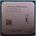
[7] The second generation desktop and laptop APU, codenamed Trinity, was announced at AMD's 2010 Financial Analyst Day[8][9] and released in October 2012.
[33] The goal is to create a "fully integrated" APU, which, according to AMD, will eventually feature 'heterogeneous cores' capable of processing both CPU and GPU work automatically, depending on the workload requirement.
[40] The AMD Brazos platform was introduced on 4 January 2011, targeting the subnotebook, netbook and low power small form factor markets.
It comprised the 4.5-watt AMD Z-Series APU (codenamed Hondo) and the A55T Fusion Controller Hub (FCH), designed for the tablet computer market.
[46] The first iteration of the second generation platform, released in October 2012, brought improvements to CPU and GPU performance to both desktops and laptops.
The platform features 2 to 4 Piledriver CPU cores built on a 32 nm process with a TDP between 65 W and 100 W, and a GPU based on the Radeon HD7000 series with support for DirectX 11, OpenGL 4.2, and OpenCL 1.2.
[53][54] They were fabricated at a 28 nm process in an FT3 ball grid array package by Taiwan Semiconductor Manufacturing Company (TSMC), and were released on 23 May 2013.
[69] Ian Cutress and Rahul Garg of Anandtech asserted that Kaveri represented the unified system-on-a-chip realization of AMD's acquisition of ATI.