Central processing unit
[3][4][5] This role contrasts with that of external components, such as main memory and I/O circuitry,[6] and specialized coprocessors such as graphics processing units (GPUs).
Modern CPUs devote a lot of semiconductor area to caches and instruction-level parallelism to increase performance and to CPU modes to support operating systems and virtualization.
[14] On June 30, 1945, before ENIAC was made, mathematician John von Neumann distributed a paper entitled First Draft of a Report on the EDVAC.
[21] Both the miniaturization and standardization of CPUs have increased the presence of digital devices in modern life far beyond the limited application of dedicated computing machines.
[29] The key difference between the von Neumann and Harvard architectures is that the latter separates the storage and treatment of CPU instructions and data, while the former uses the same memory space for both.
Clock signal frequencies ranging from 100 kHz to 4 MHz were very common at this time, limited largely by the speed of the switching devices they were built with.
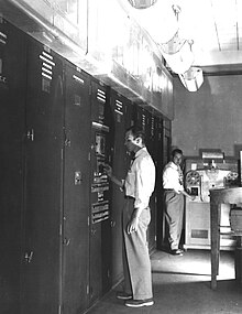
[35] With this improvement, more complex and reliable CPUs were built onto one or several printed circuit boards containing discrete (individual) components.
[42] Additionally, while discrete transistor and IC CPUs were in heavy usage, new high-performance designs like single instruction, multiple data (SIMD) vector processors began to appear.
[43] These early experimental designs later gave rise to the era of specialized supercomputers like those made by Cray Inc and Fujitsu Ltd.[43] During this period, a method of manufacturing many interconnected transistors in a compact space was developed.
To build an entire CPU out of SSI ICs required thousands of individual chips, but still consumed much less space and power than earlier discrete transistor designs.
Lee Boysel published influential articles, including a 1967 "manifesto", which described how to build the equivalent of a 32-bit mainframe computer from a relatively small number of large-scale integration circuits (LSI).
[58] The overall smaller CPU size, as a result of being implemented on a single die, means faster switching time because of physical factors like decreased gate parasitic capacitance.
This widely observed trend is described by Moore's law, which had proven to be a fairly accurate predictor of the growth of CPU (and other IC) complexity until 2016.
This section describes what is generally referred to as the "classic RISC pipeline", which is quite common among the simple CPUs used in many electronic devices (often called microcontrollers).
In others, a microprogram is used to translate instructions into sets of CPU configuration signals that are applied sequentially over multiple clock pulses.
If the resulting sum is too large (i.e., it is larger than the ALU's output word size), an arithmetic overflow flag will be set, influencing the next operation.
In modern computer designs, the control unit is typically an internal part of the CPU with its overall role and operation unchanged since its introduction.
The clock signal is produced by an external oscillator circuit that generates a consistent number of pulses each second in the form of a periodic square wave.
While it is not altogether clear whether totally asynchronous designs can perform at a comparable or better level than their synchronous counterparts, it is evident that they do at least excel in simpler math operations.
When referring to parallelism in CPUs, two terms are generally used to classify these design techniques: Each methodology differs both in the ways in which they are implemented, as well as the relative effectiveness they afford in increasing the CPU's performance for an application.
Also in case of single instruction stream, multiple data stream, a case when a lot of data from the same type has to be processed, modern processors can disable parts of the pipeline so that when a single instruction is executed many times, the CPU skips the fetch and decode phases and thus greatly increases performance on certain occasions, especially in highly monotonous program engines such as video creation software and photo processing.
In later years some of the emphasis in designing high-ILP computers has been moved out of the CPU's hardware and into its software interface, or instruction set architecture (ISA).
[80] The initial type of this technology is known as symmetric multiprocessing (SMP), where a small number of CPUs share a coherent view of their memory system.
To increase the number of cooperating CPUs beyond a handful, schemes such as non-uniform memory access (NUMA) and directory-based coherence protocols were introduced in the 1990s.
Progressively, developers refined and remade these early designs into some of the common modern SIMD specifications, which are usually associated with one instruction set architecture (ISA).
[84] Many major vendors (such as IBM, Intel, AMD, and Arm) provide software interfaces (usually written in C/C++) that can be used to collect data from the CPU's registers in order to get metrics.
[85] Operating system vendors also provide software like perf (Linux) to record, benchmark, or trace CPU events running kernels and applications.
Hardware counters provide a low-overhead method for collecting comprehensive performance metrics related to a CPU's core elements (functional units, caches, main memory, etc.)
Because of these problems, various standardized tests, often called "benchmarks" for this purpose— such as SPECint—have been developed to attempt to measure the real effective performance in commonly used applications.
[94] Due to specific capabilities of modern CPUs, such as simultaneous multithreading and uncore, which involve sharing of actual CPU resources while aiming at increased utilization, monitoring performance levels and hardware use gradually became a more complex task.