Power amplifier classes
[1] Power amplifier circuits (output stages) are classified as A, B, AB and C for linear designs—and class D and E for switching designs.
The classes are generally based on the proportion of each input cycle (conduction angle) during which an amplifying device passes current.
Because only half the waveform is amplified, significant harmonic distortion is directly present in the output signal.
Therefore, class-B amplifiers are generally operated with tuned loading - where harmonics are shorted to ground by a series of resonators.
Devices operating in Class B are used in linear amplifiers, so called because the radio frequency output power is proportional to the square of the input excitation voltage.
[15] A practical circuit using class-B elements is the push–pull stage, such as the very simplified complementary pair arrangement shown at right.
This arrangement gives good efficiency, but usually suffers from the drawback that there is a small mismatch in the cross-over region – at the "joins" between the two halves of the signal, as one output device has to take over supplying power exactly as the other finishes.
Class AB is widely considered a good compromise for amplifiers, since many types of input signal are nominally quiet enough to stay in the "class-A" region, where they are amplified with good fidelity, and by definition if passing out of this region, will be large enough that the distortion products typical of class B will be relatively small.
Often, bias voltage applied to set this quiescent current must be adjusted with the temperature of the output transistors.
(For example, in the circuit shown at right, the diodes would be mounted physically close to the output transistors, and specified to have a matched temperature coefficient.)
Another approach (often used with thermally tracking bias voltages) is to include small value resistors in series with the emitters.
The input signal is used to switch the active device, causing pulses of current to flow through a tuned circuit forming part of the load.
This is called untuned operation, and the analysis of the waveforms shows the massive distortion that appears in the signal.
The input circuit is biased so that the active element (e.g., transistor) conducts for only a fraction of the RF cycle, usually one-third (120 degrees) or less.
Ideally, the active element would pass only an instantaneous current pulse while the voltage across it is zero: it then dissipates no power and 100% efficiency is achieved.
However practical devices have a limit to the peak current they can pass, and the pulse must therefore be widened, to around 120 degrees, to obtain a reasonable amount of power, and the efficiency is then 60–70%.
The conduction angle of each device is no longer related directly to the input signal but instead varies in pulse width.
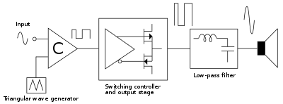
A class-D amplifier with moderate output power can be constructed using regular CMOS logic process, making it suitable for integration with other types of digital circuitry.
Thus it is commonly found in System-on-Chips with integrated audio when the amplifier shares a die with the main processor or DSP.
Though if the signal is not already in a pulse modulated format prior to amplification, it must first be converted, which may require additional circuitry.
Switching power supplies have even been modified into crude class-D amplifiers (though typically these only reproduce low-frequencies with acceptable accuracy).
Most, however, remain closer to 100 dB dynamic range at this time [2022] due to practical cost considerations.
Class-D and class-E amplifiers are sometimes mistakenly described as "digital" because the output waveform superficially resembles a pulse-train of digital symbols, but a class-D amplifier merely converts an input waveform into a continuously pulse-width modulated analog signal.
For example, class-G and class-H amplifiers are marked by variation of the supply rails (in discrete steps or in a continuous fashion, respectively) following the input signal.
Also, class-E and class-F amplifiers are commonly described in literature for radio-frequency applications where efficiency of the traditional classes is important, yet several aspects deviate substantially from their ideal values.
On the other hand, an inductive-capacitive series circuit with a large inductance and a tunable capacitance may be simpler to implement.
These amplifiers provide several power rails at different voltages and switch between them as the signal output approaches each level.
To achieve this rail tracking control, T2 and T4 act as current amplifiers, each in series with its low voltage counterpart T1 and T3.
This is because the D1 and D3 diodes which are intended to provide a path for the output voltage back into the upper devices are always reverse biased.
In place of these diodes, a voltage amplifier with gain which uses vout as its input would be needed in an actual design.