Image sensor
It does so by converting the variable attenuation of light waves (as they pass through or reflect off objects) into signals, small bursts of current that convey the information.
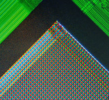
When light strikes the chip it is held as a small electrical charge in each photo sensor.
[6] Some CMOS imaging sensors also use Back-side illumination to increase the number of photons that hit the photodiode.
Another design, a hybrid CCD/CMOS architecture (sold under the name "sCMOS") consists of CMOS readout integrated circuits (ROICs) that are bump bonded to a CCD imaging substrate – a technology that was developed for infrared staring arrays and has been adapted to silicon-based detector technology.
[10] There are many parameters that can be used to evaluate the performance of an image sensor, including dynamic range, signal-to-noise ratio, and low-light sensitivity.
For sensors of comparable types, the signal-to-noise ratio and dynamic range improve as the size increases.
Electronic shuttering can be "global," in which case the entire image sensor area's accumulation of photoelectrons starts and stops simultaneously, or "rolling" in which case the exposure interval of each row immediate precedes that row's readout, in a process that "rolls" across the image frame (typically from top to bottom in landscape format).
Global electronic shuttering is less common, as it requires "storage" circuits to hold charge from the end of the exposure interval until the readout process gets there, typically a few milliseconds later.
[19] The basis for modern solid-state image sensors is MOS technology,[20][21] which originates from the invention of the MOSFET by Mohamed M. Atalla and Dawon Kahng at Bell Labs in 1959.
[23] It is a type of photodiode array, with pixels containing a p-n junction, integrated capacitor, and MOSFETs as selection transistors.
[4] These early photodiode arrays were complex and impractical, requiring selection transistors to be fabricated within each pixel, along with on-chip multiplexer circuits.
[25] The charge-coupled device (CCD) was invented by Willard S. Boyle and George E. Smith at Bell Labs in 1969.
As it was fairly straightforward to fabricate a series of MOS capacitors in a row, they connected a suitable voltage to them so that the charge could be stepped along from one to the next.
This was enabled by advances in MOS semiconductor device fabrication, with MOSFET scaling reaching smaller micron and then sub-micron levels.
The first optical mouse, invented by Richard F. Lyon at Xerox in 1980, used a 5 μm NMOS integrated circuit sensor chip.