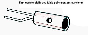
Point-contact transistor
The group had been working together on experiments and theories of electric field effects in solid state materials, with the aim of replacing vacuum tubes with a smaller device that consumed less power.
The critical experiment, carried out on December 16, 1947, consisted of a block of germanium, a semiconductor, with two very closely spaced gold contacts held against it by a spring.
While point-contact transistors usually worked fine when the metal contacts were simply placed close together on the germanium base crystal, it was desirable to obtain as high an α current gain as possible.
To obtain a higher α current gain in a point-contact transistor, a brief high-current pulse was used to modify the properties of the collector point of contact, a technique called 'electrical forming'.
While the effects of forming were understood empirically, the exact physics of the process could never be adequately studied and thus no clear theory was ever developed to explain it or provide guidance on improving it.