Power MOSFET
Compared to the other power semiconductor devices, such as an insulated-gate bipolar transistor (IGBT) or a thyristor, its main advantages are high switching speed and good efficiency at low voltages.
Generations of MOSFETs enabled power designers to achieve performance and density levels not possible with bipolar transistors.
[13] The same year, the DMOS (double-diffused MOSFET) with self-aligned gate was first reported by Y. Tarui, Y. Hayashi and Toshihiro Sekigawa of the Electrotechnical Laboratory (ETL).
[16] John Moll's research team at HP Labs fabricated DMOS prototypes in 1977, and demonstrated advantages over the VMOS, including lower on-resistance and higher breakdown voltage.
[18] Alex Lidow co-invented the HexFET, a hexagonal type of Power MOSFET, at Stanford University in 1977,[19] along with Tom Herman.
[22] David J. Coe at Philips invented the superjunction MOSFET with alternating p-type and n-type layers by filing a US patent in 1984 which was awarded in 1988.
When this highly non-symmetrical structure is reverse-biased, the space-charge region extends principally on the light-doped side, i.e., over the N− layer.
Two main parameters govern both the breakdown voltage and the RDSon of the transistor: the doping level and the thickness of the N− epitaxial layer.
However, if it were, this would result in a floating P zone between the N-doped source and drain, which is equivalent to a NPN transistor with a non-connected base.
This solution, however, creates a diode between the drain (cathode) and the source (anode) of the MOSFET, making it able to block current in only one direction.
While these diodes usually have rather high forward voltage drop, they can handle large currents and are sufficient in many applications, reducing part count, and thus, device cost and board space.
To increase efficiency, synchronous rectification is often used to minimize the amount of time that the body diode conducts current.
This can be a relatively slow process because the current that flows through the gate capacitances is limited by the external driver circuit.
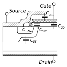
When the MOSFET is in on-state, CGDj is shunted, so the gate to drain capacitance remains equal to CoxD, a constant value.
To operate, the MOSFET must be connected to the external circuit, most of the time using wire bonding (although alternative techniques are investigated).
These connections exhibit a parasitic inductance, which is in no way specific to the MOSFET technology, but has important effects because of the high commutation speeds.
Parasitic inductances tend to maintain their current constant and generate overvoltage during the transistor turn off, resulting in increasing commutation losses.
In the datasheets, manufacturers often state a maximum gate to source voltage, around 20 V, and exceeding this limit can result in destruction of the component.
Furthermore, a high gate to source voltage reduces significantly the lifetime of the MOSFET, with little to no advantage on RDSon reduction.
Exceeding the breakdown voltage causes the device to conduct, potentially damaging it and other circuit elements due to excessive power dissipation.
The drain current is limited by heating due to resistive losses in internal components such as bond wires, and other phenomena such as electromigration in the metal layer.
The type of power dissipation, whether continuous or pulsed, affects the maximum operating temperature, due to thermal mass characteristics; in general, the lower the frequency of pulses for a given power dissipation, the higher maximum operating ambient temperature, due to allowing a longer interval for the device to cool down.
It is less efficient than a cellular structure of equivalent resolution in terms of channel density, but can cope with smaller pitch.
Another advantage of the planar stripe structure is that it is less susceptible to failure during avalanche breakdown events in which the parasitic bipolar transistor turns on from sufficient forward bias.
In the cellular structure, if the source terminal of any one cell is poorly contacted, then it becomes much more likely that the parasitic bipolar transistor latches on during an avalanche breakdown event.
Because of this, MOSFETs utilizing a planar stripe structure can only fail during avalanche breakdown due to extreme thermal stress.
The main disadvantage of this type of MOSFET is the poor on-state performance, as it uses holes as charge carriers, which have a much lower mobility than electrons.
[42] In this power MOSFET structure, also called trench-MOS, the gate electrode is buried in a trench etched in the silicon.
Especially for voltages beyond 500 V, some manufacturers, including Infineon Technologies with its CoolMOS products, have begun to use a charge compensation principle.
This process overcomes problems inherent to the multi-level epitaxial growth approach and results in extremely low on-resistance and reduced internal capacitance.