Tunnel diode
It was invented in August 1957 by Leo Esaki and Yuriko Kurose when working at Tokyo Tsushin Kogyo, now known as Sony.
[5] Robert Noyce independently devised the idea of a tunnel diode while working for William Shockley, but was discouraged from pursuing it.
The negative differential resistance in part of their operating range allows them to function as oscillators and amplifiers, and in switching circuits using hysteresis.
[11] There is also a metal-insulator-metal (MIM) diode, but due to inherent sensitivities, its present application appears to be limited to research environments.
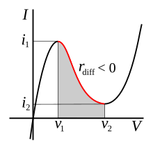
[12] Under normal forward bias operation, as voltage begins to increase, electrons at first tunnel through the very narrow P-N junction barrier and fill electron states in the conduction band on the N-side which become aligned with empty valence band hole states on the P-side of the P-N junction.
This "negative resistance" region can be exploited in a solid state version of the dynatron oscillator which normally uses a tetrode thermionic valve (vacuum tube).
The tunnel diode showed great promise as an oscillator and high-frequency threshold (trigger) device since it operated at frequencies far greater than the tetrode could: well into the microwave bands.
In 1977, the Intelsat V satellite receiver used a microstrip tunnel diode amplifier (TDA) front-end in the 14–15.5 GHz frequency band.
Writing in Nature, Esaki and coauthors state that semiconductor devices in general are extremely stable, and suggest that their shelf life should be "infinite" if kept at room temperature.