Zener diode
Diodes with a higher Zener voltage have lighter doped junctions which causes their mode of operation to involve avalanche breakdown.
Later, his work led to the Bell Labs implementation of the effect in the form of an electronic device, the Zener diode.
Unless this current is limited by external circuits, the diode may be permanently damaged due to overheating at the small (localized) areas of the semiconductor junction where avalanche breakdown conduction is occurring.
It is also worth noting that the temperature coefficient of a 4.7 V Zener diode is close to that of the emitter-base junction of a silicon transistor at around −2 mV/°C, so in a simple regulating circuit where the 4.7 V diode sets the voltage at the base of an NPN transistor (i.e. their coefficients are acting in parallel), the emitter will be at around 4 V and quite stable with temperature.
Modern designs have produced devices with voltages lower than 5.6 V with negligible temperature coefficients,[citation needed].
Under 5.6 V, where the Zener effect dominates, the IV curve near breakdown is much more rounded, which calls for more care in choosing its biasing conditions.
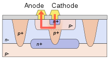
Older processes with poor control of doping characteristics had the variation of Zener voltage up to ±1 V, newer processes using ion implantation can achieve no more than ±0.25 V. The NPN transistor structure can be employed as a surface Zener diode, with collector and emitter connected together as its cathode and base region as anode.
In this approach the base doping profile usually narrows towards the surface, creating a region with intensified electric field where the avalanche breakdown occurs.
Hot carriers produced by acceleration in the intense field can inject into the oxide layer above the junction and become trapped there.
The emitter–base Zener diodes can handle only low currents as the energy is dissipated in the base depletion region which is very small.
Hot carriers then lose energy by collisions with the semiconductor lattice before reaching the oxide layer and cannot be trapped there.
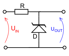
Shunt regulators are simple, but the requirements that the ballast resistor be small enough to avoid excessive voltage drop during worst-case operation (low input voltage concurrent with high load current) tends to leave a lot of current flowing in the diode much of the time, making for a fairly wasteful regulator with high quiescent power dissipation, suitable only for smaller loads.
An example of this kind of use would be a DC error amplifier used in a regulated power supply circuit feedback loop system.
Waveform clippers can be used not only to reshape a signal, but also to prevent voltage spikes from affecting circuits that are connected to the power supply.