Optical properties of carbon nanotubes
The way those materials interact with electromagnetic radiation is unique in many respects, as evidenced by their peculiar absorption, photoluminescence (fluorescence), and Raman spectra.
[1] Consequently, all the electronic, optical, electrochemical and mechanical properties of the carbon nanotubes are extremely anisotropic (directionally dependent) and tunable.
Potential applications that have been demonstrated include light emitting diodes (LEDs),[3] bolometers[4] and optoelectronic memory.
Spectroscopic methods offer the possibility of quick and non-destructive characterization of relatively large amounts of carbon nanotubes, yielding detailed measurements of non-tubular carbon content, tube type and chirality, structural defects, and many other properties that are relevant to those other applications.
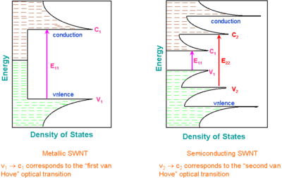
A single-walled carbon nanotubes (SWCNT) can be envisioned as strip of a graphene molecule (a single sheet of graphite) rolled and joined into a seamless cylinder.
A characteristic feature of one-dimensional crystals is that their distribution of density of states (DOS) is not a continuous function of energy, but it descends gradually and then increases in a discontinuous spike.
[11] A theoretical graph based on these calculations was designed in 1999 by Hiromichi Kataura to rationalize experimental findings.
[12] The oscillating shape of every branch of the Kataura plot reflects the intrinsic strong dependence of the SWNT properties on the (n, m) index rather than on its diameter.
While bundling strongly affects photoluminescence, it has much weaker effect on optical absorption and Raman scattering.
However, it has been recently shown that by aggregating nearly single chirality semiconducting nanotubes into closely packed Van der Waals bundles the absorption background can be attributed to free carrier transition originating from intertube charge transfer.
[16] An ideal black body should have emissivity or absorbance of 1.0, which is difficult to attain in practice, especially in a wide spectral range.
Vertically aligned "forests" of single-wall carbon nanotubes can have absorbances of 0.98–0.99 from the far-ultraviolet (200 nm) to far-infrared (200 μm) wavelengths.
Two factors could contribute to strong light absorption by these structures: (i) a distribution of CNT chiralities resulted in various bandgaps for individual CNTs.
[17][18][19] Semiconducting single-walled carbon nanotubes emit near-infrared light upon photoexcitation, described interchangeably as fluorescence or photoluminescence (PL).
Raman spectroscopy has good spatial resolution (~0.5 micrometers) and sensitivity (single nanotubes); it requires only minimal sample preparation and is rather informative.
Raman scattering in SWNTs is resonant, i.e., only those tubes are probed which have one of the bandgaps equal to the exciting laser energy.
[8] In particular, D mode is forbidden in the ideal nanotube and requires a structural defect, providing a phonon of certain angular momentum, to be induced.
The difference between those two energies, and thus the band gap of individual tubes, can be estimated from the intensity ratio of the Stokes/anti-Stokes lines.
[32] Light emitting diodes (LEDs)[3][33] and photo-detectors[34] based on a single nanotube have been produced in the lab.
Their unique feature is not the efficiency, which is yet relatively low, but the narrow selectivity in the wavelength of emission and detection of light and the possibility of its fine tuning through the nanotube structure.
In addition, bolometer[4] and optoelectronic memory[5] devices have been realised on ensembles of single-walled carbon nanotubes.
Optical properties, including the PL efficiency, can be modified by encapsulating organic dyes (carotene, lycopene, etc.)
[41] Cathodoluminescence (CL) – light emission excited by electron beam – is a process commonly observed in TV screens.