Graphene
[13] While small amounts of graphene are easy to produce using the method by which it was originally isolated, attempts to scale and automate the manufacturing process for mass production have had limited success due to cost-effectiveness and quality control concerns.
The IUPAC (International Union of Pure and Applied Chemistry) advises using the term "graphite" for the three-dimensional material and reserving "graphene" for discussions about the properties or reactions of single-atom layers.
The lack of large single crystal graphite specimens contributed to the independent development of X-ray powder diffraction by Peter Debye and Paul Scherrer in 1915, and Albert Hull in 1916.
[70] Ab initio calculations show that a graphene sheet is thermodynamically unstable if its size is less than about 20 nm and becomes the most stable fullerene (as within graphite) only for molecules larger than 24,000 atoms.
Research shows that placing hexagonal boron nitride (h-BN) in contact with graphene can alter the potential felt at atoms A and B sufficiently for the electrons to develop a mass and an accompanying band gap of about 30 meV.
[110] This permittivity, combined with its ability to function as both a conductor and as an insulator, theoretically allows compact capacitors made of graphene to store large amounts of electrical energy.
Graphene exhibits unique optical properties, showing unexpectedly high opacity for an atomic monolayer in vacuum, absorbing approximately πα ≈ 2.3% of light from visible to infrared wavelengths,[5][6][111] where α is the fine-structure constant.
[5] Based on the Slonczewski–Weiss–McClure (SWMcC) band model of graphite, calculations using Fresnel equations in the thin-film limit account for interatomic distance, hopping values, and frequency, thus assessing optical conductance.
The existence of unidirectional surface plasmons in nonreciprocal graphene-based gyrotropic interfaces has been theoretically demonstrated, offering tunability from THz to near-infrared and visible frequencies by controlling graphene's chemical potential.
[114] Particularly, the unidirectional frequency bandwidth can be 1– 2 orders of magnitude larger than that achievable with metal under similar magnetic field conditions, stemming from graphene's extremely small effective electron mass.
[117] A graphene-based Bragg grating (one-dimensional photonic crystal) has been fabricated, demonstrating its capability to excite surface electromagnetic waves in periodic structure using a 633 nm (6.33×10⁻⁷ m) He–Ne laser as the light source.
[144] Due to its large surface energy and out of plane ductility, flat graphene sheets are unstable with respect to scrolling, i.e. bending into a cylindrical shape, which is its lower-energy state.
Later in 2014, the Rice team announced that graphene showed a greater ability to distribute force from an impact than any known material, ten times that of steel per unit weight.
In a 2013 study led by James Hone's group, researchers probed the elastic stiffness and strength of CVD-grown graphene by combining nano-indentation and high-resolution TEM.
In a new study published in Nature, the researchers have used a single-layer graphene electrode and a novel surface-sensitive non-linear spectroscopy technique to investigate the top-most water layer at the electrochemically charged surface.
[201] Bilayer graphene displays the anomalous quantum Hall effect, a tunable band gap[202] and potential for excitonic condensation[203] –making it a promising candidate for optoelectronic and nanoelectronic applications.
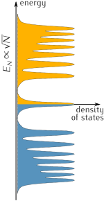
Periodically stacked graphene and its insulating isomorph provide a fascinating structural element in implementing highly functional superlattices at the atomic scale, which offers possibilities for designing nanoelectronic and photonic devices.
When adding more than one atomic layer to the barrier in each period, the coupling of electronic wavefunctions in neighboring potential wells can be significantly reduced, which leads to the degeneration of continuous subbands into quantized energy levels.
[211][212][213][214][215] Graphene nanoribbons ("nanostripes" in the "zig-zag"/"zigzag" orientation), at low temperatures, show spin-polarized metallic edge currents, which also suggests applications in the new field of spintronics.
Room temperature treatment of SLGO with carbodiimides leads to the collapse of the individual sheets into star-like clusters that exhibited poor subsequent reactivity with amines (c. 3–5% conversion of the intermediate to the final amide).
Tsinghua University in Beijing, led by Wei Fei of the Department of Chemical Engineering, claims to be able to create a carbon nanotube fiber that has a tensile strength of 80 GPa (12,000,000 psi).
[238] In 2013, researchers at Stony Brook University reported a novel radical-initiated crosslinking method to fabricate porous 3D free-standing architectures of graphene and carbon nanotubes using nanomaterials as building blocks without any polymer matrix as support.
[300][301] CVD graphene is scalable and has been grown on deposited Cu thin film catalyst on 100 to 300 mm standard Si/SiO2 wafers[302][303][304] on an Axitron Black Magic system.
[303][304] As reported by a group led by D. H. Adamson, graphene can be produced from natural graphite while preserving the integrity of the sheets using the solvent interface trapping method (SITM).
Accelerating carbon ions inside an electrical field into a semiconductor made of thin nickel films on a substrate of SiO2/Si, creates a wafer-scale (4 inches (100 mm)) wrinkle/tear/residue-free graphene layer at a relatively low temperature of 500 °C.
The Kubo formula provides an analytic expression for the graphene's conductivity and shows that it is a function of several physical parameters including wavelength, temperature, and chemical potential.
This model permits the derivation of analytical expressions for the electromagnetic field in the presence of a graphene sheet in terms of a dyadic Green function (represented using Sommerfeld integrals) and exciting electric current.
Graphene is a transparent and flexible conductor that holds great promise for various material/device applications, including solar cells,[338] light-emitting diodes (LED), integrated photonic circuit devices,[339][340] touch panels, and smart windows or phones.
[349] In January 2018, graphene-based spiral inductors exploiting kinetic inductance at room temperature were first demonstrated at the University of California, Santa Barbara, led by Kaustav Banerjee.
[361] Another review published in 2016 by Ou et al. focused on graphene-family nanomaterials (GFNs) and revealed several typical mechanisms such as physical destruction, oxidative stress, DNA damage, inflammatory response, apoptosis, autophagy, and necrosis.