Buck converter
[3] Buck converters typically operate with a switching frequency range from 100 kHz to a few MHz (citation needed).
The basic operation of the buck converter has the current in an inductor controlled by two switches (fig.
The conceptual model of the buck converter is best understood in terms of the relation between current and voltage of the inductor.
The stored energy in the inductor's magnetic field supports the current flow through the load.
The "increase" in average current makes up for the reduction in voltage, and ideally preserves the power provided to the load.
The inductor current falling below zero results in the discharging of the output capacitor during each cycle and therefore higher switching losses [de].
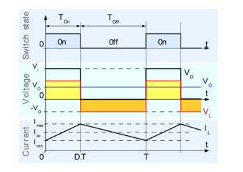
This means that the average value of the inductor voltage (VL) is zero; i.e., that the area of the yellow and orange rectangles in figure 5 are the same.
Therefore, the average value of IL can be sorted out geometrically as follows: The inductor current is zero at the beginning and rises during ton up to ILmax.
That means that ILmax is equal to: Substituting the value of ILmax in the previous equation leads to: And substituting δ by the expression given above yields: This expression can be rewritten as: It can be seen that the output voltage of a buck converter operating in discontinuous mode is much more complicated than its counterpart of the continuous mode.
The limit between discontinuous and continuous modes is reached when the inductor current falls to zero exactly at the end of the commutation cycle.
Using the notations of figure 5, this corresponds to : Therefore, the output current (equal to the average inductor current) at the limit between discontinuous and continuous modes is (see above): Substituting ILmax by its value: On the limit between the two modes, the output voltage obeys both the expressions given respectively in the continuous and the discontinuous sections.
On the circuit level, the detection of the boundary between CCM and DCM are usually provided by an inductor current sensing, requiring high accuracy and fast detectors as:[4][5] The analysis above was conducted with the assumptions: These assumptions can be fairly far from reality, and the imperfections of the real components can have a detrimental effect on the operation of the converter.
Once again, please see talk tab for more: pertaining output ripple voltage and AoE (Art of Electronics 3rd edition).
For the on-state: For the off-state: Qualitatively, as the output capacitance or switching frequency increase, the magnitude of the ripple decreases.
Output voltage ripple is typically a design specification for the power supply and is selected based on several factors.
For more accurate calculations, MOSFET datasheets contain graphs on the VDS and IDS relationship at multiple VGS values.
Observe VDS at the VGS and IDS which most closely match what is expected in the buck converter.
Switch turn-on and turn-off losses are easily lumped together as where: but this does not take into account the parasitic capacitance of the MOSFET which makes the Miller plate.
Proper selection of non-overlap time must balance the risk of shoot-through with the increased power loss caused by conduction of the body diode.
Another advantage of the synchronous converter is that it is bi-directional, which lends itself to applications requiring regenerative braking.
The simplest technique for avoiding shootthrough is a time delay between the turn-off of S1 to the turn-on of S2, and vice versa.
An improved technique for preventing this condition is known as adaptive "non-overlap" protection, in which the voltage at the switch node (the point where S1, S2 and L are joined) is sensed to determine its state.
The driver can thus adjust to many types of switches without the excessive power loss this flexibility would cause with a fixed non-overlap time.
The higher voltage drop on the low side switch is then of benefit, helping to reduce current output and meet the new load requirement sooner.
This circuit topology is used in computer motherboards to convert the 12 VDC power supply to a lower voltage (around 1 V), suitable for the CPU.
One major challenge inherent in the multiphase converter is ensuring the load current is balanced evenly across the n phases.
This technique is considered lossless because it relies on resistive losses inherent in the buck converter topology.
Voltage can be measured losslessly, across the upper switch, or using a power resistor, to approximate the current being drawn.
Switching losses happen in the transistor and diode when the voltage and the current overlap during the transitions between closed and open states.
In a complete real-world buck converter, there is also a command circuit to regulate the output voltage or the inductor current.