Bipolar junction transistor
BJTs use two p–n junctions between two semiconductor types, n-type and p-type, which are regions in a single crystal of material.
The junctions can be made in several different ways, such as changing the doping of the semiconductor material as it is grown, by depositing metal pellets to form alloy junctions, or by such methods as diffusion of n-type and p-type doping substances into the crystal.
The arrow on the symbol for bipolar transistors indicates the p–n junction between base and emitter and points in the direction in which conventional current travels.
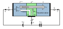
By design, most of the BJT collector current is due to the flow of charge carriers injected from a heavily doped emitter into the base where they are minority carriers (electrons in NPNs, holes in PNPs) that diffuse toward the collector, so BJTs are classified as minority-carrier devices.
When forward bias is applied to the base–emitter junction, the equilibrium between the thermally generated carriers and the repelling electric field of the emitter depletion region is disturbed.
This allows thermally excited carriers (electrons in NPNs, holes in PNPs) to inject from the emitter into the base region.
The collector–base junction is reverse-biased, and so negligible carrier injection occurs from the collector to the base, but carriers that are injected into the base from the emitter, and diffuse to reach the collector–base depletion region, are swept into the collector by the electric field in the depletion region.
The thin shared base and asymmetric collector–emitter doping are what differentiates a bipolar transistor from two separate diodes connected in series.
[6] The charge-control view easily handles phototransistors, where minority carriers in the base region are created by the absorption of photons, and handles the dynamics of turn-off, or recovery time, which depends on charge in the base region recombining.
However, because base charge is not a signal that is visible at the terminals, the current- and voltage-control views are generally used in circuit design and analysis.
In general, transistor-level circuit analysis is performed using SPICE or a comparable analog-circuit simulator, so mathematical model complexity is usually not of much concern to the designer, but a simplified view of the characteristics allows designs to be created following a logical process.
A Baker clamp can prevent the transistor from heavily saturating, which reduces the amount of charge stored in the base and thus improves switching time.
The base is physically located between the emitter and the collector and is made from lightly doped, high-resistivity material.
The collector surrounds the emitter region, making it almost impossible for the electrons injected into the base region to escape without being collected, thus making the resulting value of α very close to unity, and so, giving the transistor a large β.
The heterojunction bipolar transistor (HBT) is an improvement of the BJT that can handle signals of very high frequencies up to several hundred GHz.
[7][8] Two commonly used HBTs are silicon–germanium and aluminum gallium arsenide, though a wide variety of semiconductors may be used for the HBT structure.
For example, in the typical grounded-emitter configuration of an NPN BJT used as a pulldown switch in digital logic, the "off" state never involves a reverse-biased junction because the base voltage never goes below ground; nevertheless the forward bias is close enough to zero that essentially no current flows, so this end of the forward active region can be regarded as the cutoff region.
This applied voltage causes the lower p–n junction to become forward biased, allowing a flow of electrons from the emitter into the base.
That is, when a small change in the currents occurs, and sufficient time has passed for the new condition to reach a steady state
The bipolar point-contact transistor was invented in December 1947[11] at the Bell Telephone Laboratories by John Bardeen and Walter Brattain under the direction of William Shockley.
Nowadays, the use of the BJT has declined in favor of CMOS technology in the design of digital integrated circuits.
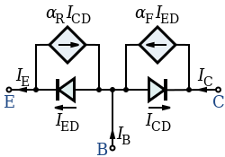
[13] BJTs can be thought of as two diodes (p–n junctions) sharing a common region that minority carriers can move through.
Both types of BJT function by letting a small current input to the base control an amplified output from the collector.
The BJT also makes a good amplifier, since it can multiply a weak input signal to about 100 times its original strength.
This two-port network is particularly suited to BJTs as it lends itself easily to the analysis of circuit behavior, and may be used to develop further accurate models.
The h refers to its being an h-parameter, a set of parameters named for their origin in a hybrid equivalent circuit model (see above).
As with all h parameters, the choice of lower case or capitals for the letters that follow the "h" is significant; lower-case signifies "small signal" parameters, that is, the slope the particular relationship; upper-case letters imply "large signal" or DC values, the ratio of the voltages or currents.
For instance, reverse breakdown of the base–emitter diode is not captured by the SGP (SPICE Gummel–Poon) model, neither are thermal effects (self-heating) or quasi-saturation.
[33] These have been addressed in various more advanced models which either focus on specific cases of application (Mextram, HICUM, Modella) or are designed for universal usage (VBIC).
So long as the pulses are short enough and infrequent enough that the device is not damaged, this effect can be used to create very sharp falling edges.


Replace x with e , b or c for CE, CB and CC topologies respectively.