CMOS
The CMOS process was presented by Fairchild Semiconductor's Frank Wanlass and Chih-Tang Sah at the International Solid-State Circuits Conference in 1963.
CMOS has since remained the standard fabrication process for MOSFET semiconductor devices in VLSI chips.
[2] Two important characteristics of CMOS devices are high noise immunity and low static power consumption.
[3] Since one transistor of the MOSFET pair is always off, the series combination draws significant power only momentarily during switching between on and off states.
Other metal gates have made a comeback with the advent of high-κ dielectric materials in the CMOS process, as announced by IBM and Intel for the 45 nanometer node and smaller sizes.
Paul Weimer, also at RCA, invented in 1962 thin-film transistor (TFT) complementary circuits, a close relative of CMOS.
[23] In 1948, Bardeen and Brattain patented the progenitor of MOSFET, an insulated-gate FET (IGFET) with an inversion layer.
Bardeen's patent, and the concept of an inversion layer, forms the basis of CMOS technology today.
[24] A new type of MOSFET logic combining both the PMOS and NMOS processes was developed, called complementary MOS (CMOS), by Chih-Tang Sah and Frank Wanlass at Fairchild.
[28] CMOS technology was initially overlooked by the American semiconductor industry in favour of NMOS, which was more powerful at the time.
[31] The first mass-produced CMOS consumer electronic product was the Hamilton Pulsar "Wrist Computer" digital watch, released in 1970.
[34] NASA's Galileo spacecraft, sent to orbit Jupiter in 1989, used the RCA 1802 CMOS microprocessor due to low power consumption.
[43] In 2000, Gurtej Singh Sandhu and Trung T. Doan at Micron Technology invented atomic layer deposition High-κ dielectric films, leading to the development of a cost-effective 90 nm CMOS process.
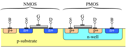
[citation needed] CMOS always uses all enhancement-mode MOSFETs (in other words, a zero gate-to-source voltage turns the transistor off).
CMOS accomplishes current reduction by complementing every nMOSFET with a pMOSFET and connecting both gates and both drains together.
However, during the switching time, both pMOS and nMOS MOSFETs conduct briefly as the gate voltage transitions from one state to another.
No matter what the input is, the output is never left floating (charge is never stored due to wire capacitance and lack of electrical drain/ground).
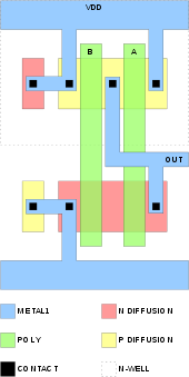
The power supply pins for CMOS are called VDD and VSS, or VCC and Ground(GND) depending on the manufacturer.
As the only configuration of the two inputs that results in a low output is when both are high, this circuit implements a NAND (NOT AND) logic gate.
On a typical ASIC in a modern 90 nanometer process, switching the output might take 120 picoseconds, and happens once every ten nanoseconds.
NMOS logic dissipates power whenever the transistor is on, because there is a current path from Vdd to Vss through the load resistor and the n-type network.
As the CMOS technology moved below sub-micron levels the power consumption per unit area of the chip has risen tremendously.
Tunnelling current becomes very important for transistors below 130 nm technology with gate oxides of 20 Å or thinner.
In modern process diode leakage is very small compared to sub threshold and tunnelling currents, so these may be neglected during power calculations.
Furthermore, recent studies have shown that leakage power reduces due to aging effects as a trade-off for devices to become slower.
[53] To speed up designs, manufacturers have switched to constructions that have lower voltage thresholds but because of this a modern NMOS transistor with a Vth of 200 mV has a significant subthreshold leakage current.
Designs (e.g. desktop processors) which include vast numbers of circuits which are not actively switching still consume power because of this leakage current.
Leakage power reduction using new material and system designs is critical to sustaining scaling of CMOS.
Parasitic transistors that are inherent in the CMOS structure may be turned on by input signals outside the normal operating range, e.g. electrostatic discharges or line reflections.
[56] RF CMOS circuits are widely used to transmit and receive wireless signals, in a variety of applications, such as satellite technology (such as GPS), bluetooth, Wi-Fi, near-field communication (NFC), mobile networks (such as 3G and 4G), terrestrial broadcast, and automotive radar applications, among other uses.