Semiconductor fabrication plant
In the microelectronics industry, a semiconductor fabrication plant, also called a fab or a foundry, is a factory where integrated circuits (ICs) are manufactured.
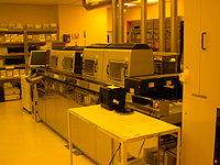
[1] The cleanroom is where all fabrication takes place and contains the machinery for integrated circuit production such as steppers and/or scanners for photolithography, etching, cleaning, and doping.
The clean room must also be damped against vibration to enable nanometer-scale alignment of photolithography machines and must be kept within narrow bands of temperature and humidity.
For many companies these older fabs are useful for producing designs for unique markets, such as embedded processors, flash memory, and microcontrollers.
The goal is to spread production costs (chemicals, fab time) over a larger number of saleable chips.
[8] Additionally, there is a large push to completely automate the production of semiconductor chips from beginning to end.
An important goal of this initiative is to enable fabs to produce greater quantities of smaller chips as a response to shorter lifecycles seen in consumer electronics.
The logic is that such a fab can produce smaller lots more easily and can efficiently switch its production to supply chips for a variety of new electronic devices.