Photolithography
Photolithography is the most common method for the semiconductor fabrication of integrated circuits ("ICs" or "chips"), such as solid-state memories and microprocessors.
Other technologies in this broader class include the use of steerable electron beams, or more rarely, nanoimprinting, interference, magnetic fields, or scanning probes.
A thin coating of the bitumen on a sheet of metal, glass or stone became less soluble where it was exposed to light; the unexposed parts could then be rinsed away with a suitable solvent, baring the material beneath, which was then chemically etched in an acid bath to produce a printing plate.
The light-sensitivity of bitumen was very poor and very long exposures were required, but despite the later introduction of more sensitive alternatives, its low cost and superb resistance to strong acids prolonged its commercial life into the early 20th century.
In 1940, Oskar Süß created a positive photoresist by using diazonaphthoquinone, which worked in the opposite manner: the coating was initially insoluble and was rendered soluble where it was exposed to light.
[7][8] At the same time Moe Abramson and Stanislaus Danko of the US Army Signal Corps developed a technique for printing circuits.
[8] In 1952, the U.S. military assigned Jay W. Lathrop and James R. Nall at the National Bureau of Standards (later the U.S. Army Diamond Ordnance Fuze Laboratory, which eventually merged to form the now-present Army Research Laboratory) with the task of finding a way to reduce the size of electronic circuits in order to better fit the necessary circuitry in the limited space available inside a proximity fuze.
[9] Inspired by the application of photoresist, a photosensitive liquid used to mark the boundaries of rivet holes in metal aircraft wings, Nall determined that a similar process can be used to protect the germanium in the transistors and even pattern the surface with light.
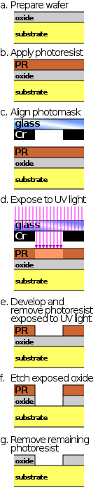
[15] If organic or inorganic contaminations are present on the wafer surface, they are usually removed by wet chemical treatment, e.g. the RCA clean procedure based on solutions containing hydrogen peroxide.
A post-exposure bake (PEB) is performed before developing, typically to help reduce standing wave phenomena caused by the destructive and constructive interference patterns of the incident light.
[34][27][35] In etching, a liquid ("wet") or plasma ("dry") chemical agent removes the uppermost layer of the substrate in the areas that are not protected by photoresist.
In semiconductor fabrication, dry etching techniques are generally used, as they can be made anisotropic, in order to avoid significant undercutting of the photoresist pattern.
This is essential when the width of the features to be defined is similar to or less than the thickness of the material being etched (i.e. when the aspect ratio approaches unity).
Wet etch processes are generally isotropic in nature, which is often indispensable for microelectromechanical systems, where suspended structures must be "released" from the underlying layer.
The development of low-defectivity anisotropic dry-etch process has enabled the ever-smaller features defined photolithographically in the resist to be transferred to the substrate material.
Research and prototyping processes often use contact or proximity lithography, because it uses inexpensive hardware and can achieve high optical resolution.
Hence, except for projection lithography (see below), contact printing offers the best resolution, because its gap distance is approximately zero (neglecting the thickness of the photoresist itself).
In addition, nanoimprint lithography may revive interest in this familiar technique, especially since the cost of ownership is expected to be low; however, the shortcomings of contact printing discussed above remain as challenges.
This data file is converted to a series of polygons and written onto a square of fused quartz substrate covered with a layer of chromium using a photolithographic process.
Where the photoresist on the mask is exposed, the chrome can be etched away, leaving a clear path for the illumination light in the stepper/scanner system to travel through.
Since the mid-1990s Cymer Inc. has become the dominant supplier of excimer laser sources to the lithography equipment manufacturers, with Gigaphoton Inc. as their closest rival.
Furthermore, insulating materials such as silicon dioxide, when exposed to photons with energy greater than the band gap, release free electrons and holes which subsequently cause adverse charging.
The liquid used is typically ultra-pure, deionised water, which provides for a refractive index above that of the usual air gap between the lens and the wafer surface.
Experimental tools using the 157 nm wavelength from the F2 excimer laser in a manner similar to current exposure systems have been built.
Mercury arc lamps are designed to maintain a steady DC current of 50 to 150 Volts, however excimer lasers have a higher resolution.
Excimer lasers are gas-based light systems that are usually filled with inert and halide gases (Kr, Ar, Xe, F and Cl) that are charged by an electric field.
In addition to running at a higher frequency, excimer lasers are compatible with more advanced machines than mercury arc lamps are.
However vacuum systems and a number of novel technologies (including much higher EUV energies than are now produced) are needed to work with UV at the edge of the X-ray spectrum (which begins at 10 nm).
Usage of these light sources have a lot of benefits, including possibility to manufacture true 3D objects and process non-photosensitized (pure) glass-like materials with superb optical resiliency.
Modern techniques using excimer laser lithography already print features with dimensions a fraction of the wavelength of light used – an amazing optical feat.