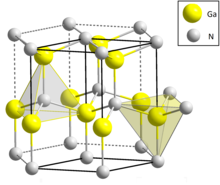
Gallium nitride
Gallium nitride (GaN) is a binary III/V direct bandgap semiconductor commonly used in blue light-emitting diodes since the 1990s.
Its wide band gap of 3.4 eV affords it special properties for applications in optoelectronics,[9][10][11] high-power and high-frequency devices.
For example, GaN is the substrate that makes violet (405 nm) laser diodes possible, without requiring nonlinear optical frequency doubling.
Its sensitivity to ionizing radiation is low (like other group III nitrides), making it a suitable material for solar cell arrays for satellites.
[13] Due to high power density and voltage breakdown limits GaN is also emerging as a promising candidate for 5G cellular base station applications.
[15] In its pure form it resists cracking and can be deposited in thin film on sapphire or silicon carbide, despite the mismatch in their lattice constants.
[17][18] However, the Si and Mg atoms change the way the GaN crystals grow, introducing tensile stresses and making them brittle.
[19] Gallium nitride compounds also tend to have a high dislocation density, on the order of 108 to 1010 defects per square centimeter.
[21] Scientists at ARL experimentally obtained a peak steady-state velocity of 1.9×107 cm/s, with a transit time of 2.5 picoseconds, attained at an electric field of 225 kV/cm.
The first GaN-based high-brightness LEDs used a thin film of GaN deposited via metalorganic vapour-phase epitaxy (MOVPE) on sapphire.
The first gallium nitride metal semiconductor field-effect transistors (GaN MESFET) were experimentally demonstrated in 1993[30] and they are being actively developed.
These transistors are built by growing a thin layer of GaN on top of a standard silicon wafer, often referred to as GaN-on-Si by manufacturers.
Another seemingly viable solution for realizing enhancement-mode GaN-channel HFETs is to employ a lattice-matched quaternary AlInGaN layer of acceptably low spontaneous polarization mismatch to GaN.
[34] [35] Integration means that the gate-drive loop has essentially zero impedance, which further improves efficiency by virtually eliminating FET turn-off losses.
Academic studies into creating low-voltage GaN power ICs began at the Hong Kong University of Science and Technology (HKUST) and the first devices were demonstrated in 2015.
GaN-based electronics (not pure GaN) have the potential to drastically cut energy consumption, not only in consumer applications but even for power transmission utilities.
Polishing methods typically employ a liquid electrolyte and UV irradiation to enable mechanical removal of a thin oxide layer from the wafer.