Celeron
They typically offer less performance per clock speed compared to flagship Intel CPU lines, such as the Pentium or Core brands.
As a product concept, the Celeron was introduced in response to Intel's loss of the low-end market, in particular to the Cyrix 6x86, the AMD K6, and the IDT Winchip.
The Celeron also effectively killed off the nine-year-old 80486 chip, which had been the low-end processor brand for entry-level desktops and laptops until 1998.
The San Jose Mercury News described Lexicon's reasoning behind the name they chose: "Celer is Latin for swift, as in the word 'accelerate', and 'on' as in 'turned on'.
[3] Substantial numbers were sold on first release, largely on the strength of the Intel name, but the Celeron quickly achieved a poor reputation both in the trade press and among computer professionals.
[6] The initial market interest faded rapidly in the face of its poor performance, and with sales at a very low level, Intel felt obliged to develop a substantially faster replacement as soon as possible.
Indeed, most industry analysts regarded the first Mendocino-based Celerons as too successful—performance was sufficiently high to not only compete strongly with rival parts, but also to attract buyers away from Intel's high-profit flagship, the Pentium II.
[7] Some motherboards were designed to prevent this modification, by restricting the Celeron's front side bus to 66 MHz.
However, overclockers soon found that putting tape over pin B21 of the Celeron's interface slot circumvented this, allowing a 100 MHz bus.
[8] At the time on-die cache was difficult to manufacture; especially L2 as more of it is needed to attain an adequate level of performance.
The Pentium II's 512 KB of L2 cache was implemented with a pair of relatively high-performance L2 cache chips mounted on a special-purpose board alongside the processor itself, running at half the processor's clock rate and communicating with the CPU through a special back-side bus.
The Mendocino Celeron CPU came only designed for a 66 MHz front-side bus, but this would not be a serious performance bottleneck until clock rates reached higher levels.
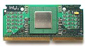
The Slot 1 form had been designed to accommodate the off-chip cache of the Pentium II and had mounting problems with motherboards.
One interesting note about the PPGA Socket 370 Mendocinos is they supported symmetric multiprocessing (SMP), and there was at least one motherboard released (the ABIT BP6) which took advantage of this fact.
These Celeron processors, released initially at 1.2 GHz on October 2, 2001,[14] were based on the Pentium III 'Tualatin' core and made with a 0.13 micrometer process for the FCPGA 2 Socket 370.
[citation needed] On the other hand, this improved stability when overclocking and most of them had no problem working at 133 MHz FSB for a substantial performance increase.
The only difference between the Northwood-128-based and the Willamette-128-based Celeron is the fact that it was built on the new 130 nm process which shrank the die size, increased the transistor count, and lowered the core voltage from 1.7 V on the Willamette-128 to 1.52 V for the Northwood-128.
Unlike the fairly cool-running Northwood Celeron, the Prescott-256 had a class-rated TDP of 73 W, which prompted Intel to include a more intricate copper core/aluminum finned cooler to help handle the additional heat.
The Cedar Mill Celeron D is largely the same as the Prescott-256, except with double the L2 cache (512 KB) and based on a 65 nm manufacturing process.
The CPU has 800 MT/s FSB, 65 W TDP and uses 512 KB of the chip's 2 MB L2 cache, significantly limiting performance for uses such as gaming.
The main difference to Allendale-based Celeron processors is the support for Intel VT-x and increased performance due to the double L2 Cache of 1 MB.
Despite using the same Clarkdale chip as the Core i5-6xx line, it does not support Turbo Boost, HyperThreading, VT-d, SMT, Trusted Execution Technology or AES new instructions, and it comes with only 2 MB of third-level cache enabled.
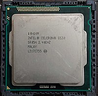
They are LGA 1155 processors (available in single- and dual-core versions) with integrated Intel HD Graphics GPU and containing up to 2 MB of L3 cache.
They give some boost in performance over Sandy Bridge-based Celerons due to a 22 nm die shrink, as well as some other minor improvements.
These Celeron processors were a good deal higher performing than the desktop counterparts because of their larger L2 cache sizes.
A system based on the Celeron M processor may not use the Centrino brand name, regardless of what chipset and Wi-Fi components are used.
It is used in Intel's small form factor D845GVSH motherboard, intended for Asian and South American markets.
The platform consists of a 945GSE chipset, which includes built-in DirectX 9 graphics and supports single channel DDR2 memory.
An 802.11g Wi-Fi module, USB/PATA port SSD (solid state drive), and a 7- or 8-inch panel will typically round out the platform.
This core also brings new features to Celeron M including a higher front side bus (533 MT/s), SSE3 instructions.