Invention of the integrated circuit
Between 1953 and 1957, Sidney Darlington and Yasuo Tarui (Electrotechnical Laboratory) proposed similar chip designs where several transistors could share a common active area, but there was no electrical isolation to separate them from each other.
[2][3] He invented a way to connect the IC components (aluminium metallization) and proposed an improved version of insulation based on the planar process technology developed by Jean Hoerni.
[4] In the 2000s, historians Leslie Berlin,[a] Bo Lojek[b] and Arjun Saxena[c] reinstated the idea of multiple IC inventors and revised the contribution of Kilby.
[1] During and immediately after World War II a phenomenon named "the tyranny of numbers" was noticed, that is, some computational devices reached a level of complexity at which the losses from failures and downtime exceeded the expected benefits.
On May 7, 1952, the British radio engineer Geoffrey Dummer formulated the idea of integration in a public speech in Washington: With the advent of the transistor and the work in semiconductors generally, it seems now to be possible to envisage electronic equipment in a solid block with no connecting wires.
[19][20] On May 21, 1953, Harwick Johnson filed a patent application for a method of forming various electronic components – transistors, resistors, lumped and distributed capacitances – on a single chip.
[30] Only in the summer of 1959, after the inventions of Kilby, Lehovec and Hoerni became publicly known, D'Asaro reported an operational shift register based on silicon thyristors.
[28] The failures of Shockley, Ross and Wallmark proved the fallacy of this approach: the mass production of functional devices was hindered by technological barriers.
[32] Also in 1954, Fuller and Dittsenberger published a fundamental study of diffusion in silicon, and Shockley suggested using this technology to form p-n junctions with a given profile of the impurity concentration.
[51][52] On September 12, he presented the first IC prototype,[48] which was a single-transistor oscillator with a distributed RC feedback, repeating the idea and the circuit in the 1953 patent by Johnson.
[66][67] Kilby's colleague Harvey Cragon packed this computer into a volume of a little over 100 cm3, using 587 ICs to replace around 8,500 transistors and other components that would be needed to perform the equivalent function.
[61] In late 1958, Kurt Lehovec, a scientist working at the Sprague Electric Company, attended a seminar at Princeton where Wallmark outlined his vision of the fundamental problems in microelectronics.
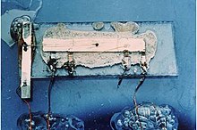
His device was a linear structure 2.2×0.5×0.1 mm in size, which was divided into isolated n-type cells (bases of the future transistors) by p-n junctions.
[71] On January 14, 1959, Jean Hoerni introduced his latest version of the planar process to Robert Noyce and a patent attorney John Rallza at Fairchild Semiconductor.
The first photolithography step aims to open windows corresponding to the planned devices, and diffuse impurities to create low-resistance "wells" through the entire thickness of the chip.
However, Kilby favored thick coating layers of different metals (aluminium, copper or antimony-doped gold) and silicon monoxide instead of the dioxide.
[109] General Microelectronics later introduced the first commercial MOS integrated circuit in 1964,[110] a 120-transistor shift register developed by Robert Norman.
The situation changed in 1962 when Texas Instruments started to zealously pursue the real and imaginary infringers of their patents and received the nicknames "The Dallas legal firm"[111] and "semiconductor cowboys".
[113] In the early 1960s, the US Appeals Court ruled that Noyce was the inventor of the monolithic integrated circuit chip based on adherent oxide and junction isolation technologies.
Four years later, Texas Instruments hosted in Dallas an arbitration hearing with demonstrations of the Kilby's inventions and depositions by experts.
Hughes acquired the rights to one of the seventeen points of the Hoerni's patent, and then exchanged it for a small percentage of the future licensing incomes of Fairchild.
By 1965, the planar technology of Fairchild became the industry standard, but the license to patents of Hoerni and Noyce was purchased by less than ten manufacturers, and there were no mechanisms to pursue unlicensed production.
[124] For two years MITI did not give a definite answer to the request, and in 1965 Texas Instruments retaliated by threatening with embargo on the import of electronic equipment that infringed their patents.
[130] Sorab Ghandhi in "Theory and Practice of Microelectronics" (1968) wrote that the patents of Lehovec and Hoerni were the high point of semiconductor technology of the 1950s and opened the way for the mass production of ICs.
[131] In October 1966, Kilby and Noyce were awarded the Ballantine Medal from the Franklin Institute "for their significant and essential contribution to the development of integrated circuits".
Texas Instruments picked his name because it stood on the patent they challenged and thereby "appointed" him as a sole representative of all the development work at Fairchild.
[138] Robert Wright of The New York Times criticized Reid for a lengthy description of the supporting characters involved in the invention,[139] yet the contributions of Lehovec and Last were not mentioned, and Jean Hoerni appears in the book only as a theorist who consulted Noyce.
[138] Paul Ceruzzi in "A History of Modern Computing" (2003) also repeated the two-inventor story and stipulated that "Their invention, dubbed at first Micrologic, then the Integrated Circuit by Fairchild, was simply another step along this path" (of miniaturization demanded by the military programs of the 1950s).
[145] Fred Kaplan in his popular book "1959: The Year Everything Changed" (2010) spends eight pages on the IC invention and assigns it to Kilby,[146] mentioning Noyce only in a footnote[147] and neglecting Hoerni and Last.
In 1998, Michael Riordan and Lillian Hoddson detailed the events leading to the invention of Kilby in "Crystal Fire: The Birth of the Information Age".


