Memory cell (computing)
The SRAM (static RAM) memory cell is a type of flip-flop circuit, typically implemented using MOSFETs.
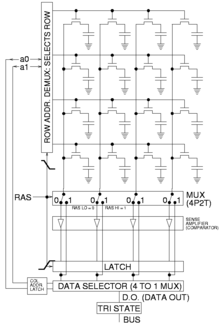
Due to this refresh process, DRAM consumes more power, but it can achieve higher storage densities.
[2] Logic circuits without memory cells are called combinational, meaning the output depends only on the present input.
In computers, it allows to store both programs and data and memory cells are also used for temporary storage of the output of combinational circuits to be used later by digital systems.
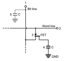
Since the DRAM memory cell stores its value as the charge of a capacitor, and there are current leakage issues, its value must be constantly rewritten.
That is the reason why SRAM memory is used for on-chip cache included in modern microprocessor chips.
[5] In that year, the first patent applications for magnetic-core memory were filed by Frederick Viehe.
[6][7] Practical magnetic-core memory was developed by An Wang in 1948, and improved by Jay Forrester and Jan A. Rajchman in the early 1950s, before being commercialised with the Whirlwind computer in 1953.
[12][13] The invention of the MOSFET enabled the practical use of metal–oxide–semiconductor (MOS) transistors as memory cell storage elements, a function previously served by magnetic cores.
In 1966, Robert H. Dennard at the IBM Thomas J. Watson Research Center was working on MOS memory.
[20] In 1967, Dennard filed a patent for a single-transistor DRAM memory cell, based on MOS technology.
One year later, it released the first DRAM integrated circuit chip, the Intel 1103, based on MOS technology.
[25] The floating-gate MOSFET (FGMOS) was invented by Dawon Kahng and Simon Sze at Bell Labs in 1967.
[29] According to R. Bez and A. Pirovano: A floating-gate memory cell is basically an MOS transistor with a gate completely surrounded by dielectrics (Fig.
Charge injected into the FG is maintained there, allowing modulation of the ‘apparent’ threshold voltage (i.e. VT seen from the CG) of the cell transistor.


(A) S = 1, R = 0: set
(B) S = 0, R = 0: hold
(C) S = 0, R = 1: reset
(D) S = 1, R = 1: not allowed
Transitioning from the restricted combination (D) to (A) leads to an unstable state.
