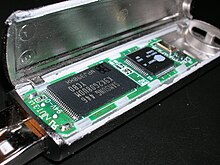
Flash memory
NAND or NOR flash memory is also often used to store configuration data in digital products, a task previously made possible by EEPROM or battery-powered static RAM.
[11][12] The original MOSFET was invented at Bell Labs between 1955 and 1960, after Frosch and Derick discovered surface passivation and used their discovery to create the first planar transistors.
[31] NOR-based flash has long erase and write times, but provides full address and data buses, allowing random access to any memory location.
This makes it a suitable replacement for older read-only memory (ROM) chips, which are used to store program code that rarely needs to be updated, such as a computer's BIOS or the firmware of set-top boxes.
This makes NAND flash unsuitable as a drop-in replacement for program ROM, since most microprocessors and microcontrollers require byte-level random access.
NAND flash has achieved significant levels of memory density as a result of several major technologies that were commercialized during the late 2000s to early 2010s.
[37] In 2009, Toshiba and SanDisk introduced NAND flash chips with QLC technology storing 4 bits per cell and holding a capacity of 64 Gbit.
[41][42][43][44][45][46] Because CTF replaces the polysilicon with an electrically insulating nitride, it allows for smaller cells and higher endurance (lower degradation or wear).
In 1991, NEC researchers including N. Kodama, K. Oyama and Hiroki Shirai described a type of flash memory with a charge trap method.
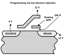
Degradation or wear (and the limited endurance of floating gate Flash memory) occurs due to the extremely high electric field (10 million volts per centimeter) experienced by the oxide.
Such high voltage densities can break atomic bonds over time in the relatively thin oxide, gradually degrading its electrically insulating properties and allowing electrons to be trapped in and pass through freely (leak) from the floating gate into the oxide, increasing the likelihood of data loss since the electrons (the quantity of which is used to represent different charge levels, each assigned to a different combination of bits in MLC Flash) are normally in the floating gate.
[citation needed] The low read latencies characteristic of NOR devices allow for both direct code execution and data storage in a single memory product.
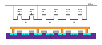
Despite the additional transistors, the reduction in ground wires and bit lines allows a denser layout and greater storage capacity per chip.
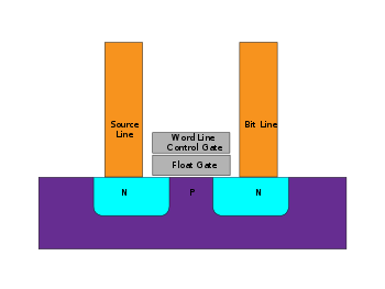
The hierarchical structure of NAND flash starts at a cell level which establishes strings, then pages, blocks, planes and ultimately a die.
[91] As of 2013,[update] V-NAND flash architecture allows read and write operations twice as fast as conventional NAND and can last up to 10 times as long, while consuming 50 percent less power.
Although data structures in flash memory cannot be updated in completely general ways, this allows members to be "removed" by marking them as invalid.
[103][104] Micron Technology and Sun Microsystems announced an SLC NAND flash memory chip rated for 1,000,000 P/E cycles on 17 December 2008.
This limitation also exists for "read-only" applications such as thin clients and routers, which are programmed only once or at most a few times during their lifetimes, due to read disturb (see below).
[127] The goal of the group is to provide standard software and hardware programming interfaces for nonvolatile memory subsystems, including the "flash cache" device connected to the PCI Express bus.
[143] However, by applying certain algorithms and design paradigms such as wear leveling and memory over-provisioning, the endurance of a storage system can be tuned to serve specific requirements.
Multiple chips are often arrayed or die stacked to achieve higher capacities[175] for use in consumer electronic devices such as multimedia players or GPSs.
It is considerably larger than the advertised capacity in order to allow for distribution of writes (wear leveling), for sparing, for error correction codes, and for other metadata needed by the device's internal firmware.
Since this type of SPI flash lacks an internal SRAM buffer, the complete block must be read out and modified before being written back, making it slow to manage.
Typical applications for serial NOR flash include storing firmware for hard drives, BIOS, Option ROM of expansion cards, DSL modems, etc.
For relational databases or other systems that require ACID transactions, even a modest amount of flash storage can offer vast speedups over arrays of disk drives.
[193] The first flash-memory based PC to become available was the Sony Vaio UX90, announced for pre-order on 27 June 2006 and began to be shipped in Japan on 3 July 2006 with a 16 GB flash memory hard drive.
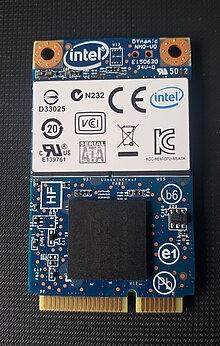
Starting in late 2011, as part of Intel's Ultrabook initiative, an increasing number of ultra-thin laptops are being shipped with SSDs standard.
[197] It is unclear how long data on flash memory will persist under archival conditions (i.e., benign temperature and humidity with infrequent access with or without prophylactic rewrite).
Due to its relatively simple structure and high demand for higher capacity, NAND flash memory is the most aggressively scaled technology among electronic devices.
The heavy competition among the top few manufacturers only adds to the aggressiveness in shrinking the floating-gate MOSFET design rule or process technology node.