Nanoelectronics
The term covers a diverse set of devices and materials, with the common characteristic that they are so small that inter-atomic interactions and quantum mechanical properties need to be studied extensively.
The field of nanoelectronics aims to enable the continued realization of this law by using new methods and materials to build electronic devices with feature sizes on the nanoscale.
For this reason, while super-miniature electronic integrated circuits are fully functional, the same technology cannot be used to make working mechanical devices beyond the scales where frictional forces start to exceed the available power.
So even though you may see microphotographs of delicately etched silicon gears, such devices are currently little more than curiosities with limited real world applications, for example, in moving mirrors and shutters.
This could possibly make any kind of "micro factory" impractical: even if robotic arms and hands could be scaled down, anything they pick up will tend to be impossible to put down.
The above being said, molecular evolution has resulted in working cilia, flagella, muscle fibers and rotary motors in aqueous environments, all on the nanoscale.
[3][4] Of particular prominence in this field, Silicon nanowires are being increasingly studied towards diverse applications in nanoelectronics, energy conversion and storage.
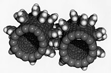
These schemes would make heavy use of molecular self-assembly, designing the device components to construct a larger structure or even a complete system on their own.
A promising application of molecular electronics was proposed by the IBM researcher Ari Aviram and the theoretical chemist Mark Ratner in their 1974 and 1988 papers Molecules for Memory, Logic and Amplification (see unimolecular rectifier).
Nanoelectronics holds the promise of making computer processors more powerful than are possible with conventional semiconductor fabrication techniques.
A number of approaches are currently being researched, including new forms of nanolithography, as well as the use of nanomaterials such as nanowires or small molecules in place of traditional CMOS components.
However, research into crossbar switch based electronics have offered an alternative using reconfigurable interconnections between vertical and horizontal wiring arrays to create ultra high density memories.
The GMR effect has led to a strong increase in the data storage density of hard disks and made the gigabyte range possible.
[citation needed] Photonic crystals are materials with a periodic variation in the refractive index with a lattice constant that is half the wavelength of the light used.
[15] However, this estimate is only true if all food was converted to electricity, and the human body needs some energy consistently, so possible power generated is likely much lower.
There is great interest in constructing nanoelectronic devices[16][17][18] that could detect the concentrations of biomolecules in real time for use as medical diagnostics,[19] thus falling into the category of nanomedicine.
Such miniaturization on nanoelectronics towards in vivo proteomic sensing should enable new approaches for health monitoring, surveillance, and defense technology.