Field-effect transistor
FETs control the current by the application of a voltage to the gate, which in turn alters the conductivity between the drain and source.
Field effect transistors generally display very high input impedance at low frequencies.
The transistor effect was later observed and explained by John Bardeen and Walter Houser Brattain while working under William Shockley at Bell Labs in 1947, shortly after the 17-year patent expired.
Shockley initially attempted to build a working FET by trying to modulate the conductivity of a semiconductor, but was unsuccessful, mainly due to problems with the surface states, the dangling bond, and the germanium and copper compound materials.
[4] The static induction transistor (SIT), a type of JFET with a short channel, was invented by Japanese engineers Jun-ichi Nishizawa and Y. Watanabe in 1950.
[6] Junction transistors were relatively bulky devices that were difficult to manufacture on a mass-production basis, which limited them to a number of specialised applications.
The insulated-gate field-effect transistor (IGFET) was theorized as a potential alternative to junction transistors, but researchers were unable to build working IGFETs, largely due to the troublesome surface state barrier that prevented the external electric field from penetrating into the material.
[6] By the mid-1950s, researchers had largely given up on the FET concept, and instead focused on bipolar junction transistor (BJT) technology.
[7] The foundations of MOSFET technology were laid down by the work of William Shockley, John Bardeen and Walter Brattain.
Based on his theory, in 1948 Bardeen patented the progenitor of MOSFET, an insulated-gate FET (IGFET) with an inversion layer.
In 1976 Shockley described Bardeen's surface state hypothesis "as one of the most significant research ideas in the semiconductor program".
In late 1947, Robert Gibney and Brattain suggested the use of electrolyte placed between metal and semiconductor to overcome the effects of surface states.
Lillian Hoddeson argues that "had Brattain and Bardeen been working with silicon instead of germanium they would have stumbled across a successful field effect transistor".
[8][9][10][11][12] By the end of the first half of the 1950s, following theoretical and experimental work of Bardeen, Brattain, Kingston, Morrison and others, it became more clear that there were two types of surface states.
Their further work demonstrated how to etch small openings in the oxide layer to diffuse dopants into selected areas of the silicon wafer.
In February 1957, John Wallmark filed a patent for FET in which germanium monoxide was used as a gate dielectric, but he didn't pursue the idea.
[30][31] With its high scalability,[32] and much lower power consumption and higher density than bipolar junction transistors,[33] the MOSFET made it possible to build high-density integrated circuits.
[41] The concept of a double-gate thin-film transistor (TFT) was proposed by H. R. Farrah (Bendix Corporation) and R. F. Steinberg in 1967.
[42] A double-gate MOSFET was first demonstrated in 1984 by Electrotechnical Laboratory researchers Toshihiro Sekigawa and Yutaka Hayashi.
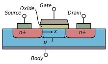
[47] The device consists of an active channel through which charge carriers, electrons or holes, flow from the source to the drain.
This gate permits electrons to flow through or blocks their passage by creating or eliminating a channel between the source and drain.
In an n-channel "enhancement-mode" device, a conductive channel does not exist naturally within the transistor, and a positive gate-to-source voltage is necessary to create one.
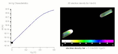
Further gate-to-source voltage increase will attract even more electrons towards the gate which are able to create an active channel from source to drain; this process is called inversion.
Even though the conductive channel formed by gate-to-source voltage no longer connects source to drain during saturation mode, carriers are not blocked from flowing.
Because base current noise will increase with shaping time[clarification needed],[68] a FET typically produces less noise than a bipolar junction transistor (BJT), and is found in noise-sensitive electronics such as tuners and low-noise amplifiers for VHF and satellite receivers.
[69] The fragile insulating layer of the MOSFET between the gate and the channel makes it vulnerable to electrostatic discharge or changes to threshold voltage during handling.
FET circuits can therefore require very careful layout and can involve trades between switching speed and power dissipation.
[70] Field-effect transistors are relatively robust, especially when operated within the temperature and electrical limitations defined by the manufacturer (proper derating).
The CMOS (complementary metal oxide semiconductor) process technology is the basis for modern digital integrated circuits.
Source-gated transistors are more robust to manufacturing and environmental issues in large-area electronics such as display screens, but are slower in operation than FETs.