Synchronous dynamic random-access memory
In SDRAM families standardized by JEDEC, the clock signal controls the stepping of an internal finite-state machine that responds to incoming commands.
This allows SDRAMs to achieve greater concurrency and higher data transfer rates than asynchronous DRAMs could.
[1][2] In the late 1980s IBM invented DDR SDRAM, they built a dual-edge clocking RAM and presented their results at the International Solid-State Circuits Convention in 1990.
Indeed, early SDRAM was somewhat slower than contemporaneous burst EDO DRAM due to the additional logic.
The benefits of SDRAM's internal buffering come from its ability to interleave operations to multiple banks of memory, thereby increasing effective bandwidth.
In operation, CAS latency is a specific number of clock cycles programmed into the SDRAM's mode register and expected by the DRAM controller.
In response, Intel published the PC100 standard, which outlines requirements and guidelines for producing a memory module that can operate reliably at 100 MHz.
Activation requires a minimum amount of time, called the row-to-column delay, or tRCD before reads or writes to it may occur.
A write command is accompanied by the data to be written driven on to the DQ lines during the same rising clock edge.
To transfer a 64-byte cache line requires eight consecutive accesses to a 64-bit DIMM, which can all be triggered by a single read or write command by configuring the SDRAM chips, using the mode register, to perform eight-word bursts.
For the sequential burst mode, later words are accessed in increasing address order, wrapping back to the start of the block when the end is reached.
However, to simplify the memory controller, SDRAM chips support an "auto refresh" command, which performs these operations to one row in each bank simultaneously.
The third, implemented in Mobile DDR (LPDDR) and LPDDR2 is "deep power down" mode, which invalidates the memory and requires a full reinitialization to exit from.
DDR SDRAM employs prefetch architecture to allow quick and easy access to multiple data words located on a common physical row in the memory.
Traditional DRAM architectures have long supported fast column access to bits on an open row.
Prefetch architecture simplifies this process by allowing a single address request to result in multiple data words.
In a prefetch buffer architecture, when a memory access occurs to a row the buffer grabs a set of adjacent data words on the row and reads them out ("bursts" them) in rapid-fire sequence on the IO pins, without the need for individual column address requests.
For instance, in DDR1, two adjacent data words will be read from each chip in the same clock cycle and placed in the pre-fetch buffer.
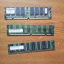
PC66 is Synchronous DRAM operating at a clock frequency of 66.66 MHz, on a 64-bit bus, at a voltage of 3.3 V. PC66 is available in 168-pin DIMM and 144-pin SO-DIMM form factors.
PC100 refers to Synchronous DRAM operating at a clock frequency of 100 MHz, on a 64-bit-wide bus, at a voltage of 3.3 V. PC100 is available in 168-pin DIMM and 144-pin SO-DIMM form factors.
PC133 refers to SDR SDRAM operating at a clock frequency of 133 MHz, on a 64-bit-wide bus, at a voltage of 3.3 V. PC133 is available in 168-pin DIMM and 144-pin SO-DIMM form factors.
PC133 is the fastest and final SDR SDRAM standard ever approved by the JEDEC, and delivers a bandwidth of 1.066 GB per second ([133.33 MHz * 64/8]=1.066 GB/s).
The DDR interface accomplishes this by reading and writing data on both the rising and falling edges of the clock signal.
DDR SDRAM (sometimes called DDR1 for greater clarity) doubles the minimum read or write unit; every access refers to at least two consecutive words.
DDR2 SDRAM is now available at a clock rate of 533 MHz generally described as DDR2-1066 and the corresponding DIMMs are known as PC2-8500 (also named PC2-8600 depending on the manufacturer).
VCM was a proprietary type of SDRAM that was designed by NEC, but released as an open standard with no licensing fees.
Unlike a normal SDRAM write, which must be performed to an active (open) row, the VCSDRAM bank must be precharged (closed) when the restore command is issued.
[35] The earliest known commercial device to use SGRAM is Sony's PlayStation (PS) video game console, starting with the Japanese SCPH-5000 model released in December 1995, using the NEC μPD481850 chip.
Their primary characteristics are higher clock frequencies for both the DRAM core and I/O interface, which provides greater memory bandwidth for GPUs.
[38] High Bandwidth Memory (HBM) is a high-performance RAM interface for 3D-stacked SDRAM from Samsung, AMD and SK Hynix.