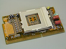
Socket 370
Socket 370 started out as a budget-oriented platform for 66 MHz FSB PPGA Mendocino Celeron CPUs in late 1998, as the move to on-die L2 cache eliminated the need for a PCB design as seen on Slot 1.
In 2001, the FC-PGA2 Tualatin Pentium III processors brought changes to the infrastructure which required dedicated Tualatin-compatible motherboards; some manufacturers would indicate this with a blue (instead of white) socket.
These late sockets were typically compatible with Coppermine processors, but not the older Mendocino Celerons.
Most Intel Socket 370 processors (Pentium III and Celeron) had mechanical maximum load limits which were designed not be exceeded during heat sink assembly, shipping conditions, or standard use.
All Intel Socket 370 processors with integrated heat sink (Pentium III and Celeron 1.13–1.4 GHz) had mechanical maximum load limits which were designed not be exceeded during heat sink assembly, shipping conditions, or standard use.