Surface imperfections (optics)
Tighter specifications increase the costs of fabricating optical elements but looser ones affect performance.
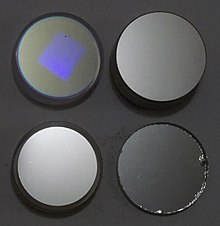
Optics for laser applications are more sensitive to surface quality as any imperfections can lead to laser-induced damage.
Optical systems requiring high radiation intensity tend to be sensitive to any loss of power due to surface scattering caused by imperfections.
There are many different standards used by optical element manufacturers, designers, and users which vary by geographic region and industry.
For example, German manufacturers use ISO 10110, while the US military developed MIL-PRF-13830 and their long-standing use of it has made it the de facto global standard.
[4] Examining surface quality in terms of 'Scratch & Dig' is a specialized skill that takes time to develop.
[3] Automated systems now replace the human technician, for flat optics, but recently also for convex and concave lenses.
A dig is defined as a pit, a rough area, or a small crater on the surface of the glass (or any other optical material).
Texture is a periodical phenomenon with a high spatial frequency (or in other words, in small dimensions), which affects the entire surface and causes the scattering of incident light.
For example, the grade that must be required outside the clear aperture (the part of the lens to which the standard applies, also called "effective diameter" or CA) is, in the absence of another definition, 80-50.
[1] Accumulation and concentration rules regulate common situations in which there are multiple defects on the surface of an optical element, and clarify how they should be added up.
[2][8] The number of digs at the maximum permitted level is determined by dividing the measured clear aperture diameter (in millimeters) by 20, and rounding up.
[4] A fundamental advantage of ISO is a relatively simple translation between the percentage of light scattered from a surface and the characterization of its surface, according to the formula:[4] Scatter % = 4 x [(N x A2)+(N' x A'2)+ N" x A" x Φ]/(π x Φ2) Unlike MIL-PRF-13830B which is cheap and fast to use, but suffers from inaccuracies, the use of the dimensional standard of ISO 10110-7 is more accurate but takes a longer time to test and is therefore expensive.
[2] The relatively long test time is derived from the fact that testing according to this standard is carried out using a microscope, comparing sizes of each defect to defects on a master, and because of the large magnification needed the field of view is small, requiring several measurements to map each optical element.
This method takes advantage of the speed and low cost of the visual inspection and is used for elements with looser tolerances.
This standard is intended for parts with tight surface quality tolerances, such as CCD cover glasses or demanding laser applications.
[1] This standard allows a relatively easy translation between the desired scattering level and the surface quality, as mentioned above.
[1] This standard replaced MIL-STD-10A and defines more than forty different parameters including RMS (root mean square), slope, skew, PSD (Power Spectral Density, which is the most comprehensive characteristic), and more.
There is a significant improvement in this standard because it allows the characterization of machined surfaces, at different spatial frequencies, which is especially important in cases where the optics were produced using techniques that leave periodic marks, such as caused by diamond turning.
This popular standard, similar to ASME B46.1, also defines the RMS of the surface over a specific length scale, PSD and more.