History of the transistor
Electrons in the emitters, or the "holes" in the collectors, would cluster at the surface of the crystal, where they could find their opposite charge "floating around" in the air (or water).
He joined the germanium effort at Purdue University in November 1943 and was given the tricky task of measuring the spreading resistance at the metal–semiconductor contact.
We might not necessarily have gone ahead and said, 'Let's start making transistors,' open up a factory and sell them... At that time the important device was the high back voltage rectifier".
[15] Shockley's research team initially attempted to build a field-effect transistor (FET), by trying to modulate the conductivity of a semiconductor, but was unsuccessful, mainly due to problems with the surface states, the dangling bond, and the germanium and copper compound materials.
In the course of trying to understand the mysterious reasons behind their failure to build a working FET, this led them to instead inventing the bipolar point-contact and junction transistors.
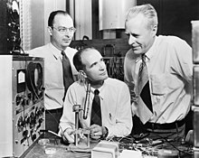
[19] Brattain and H. R. Moore made a demonstration to several of their colleagues and managers at Bell Labs on the afternoon of 23 December 1947, often given as the birth date of the transistor.
In 1956 John Bardeen, Walter Houser Brattain, and William Bradford Shockley were honored with the Nobel Prize in Physics "for their researches on semiconductors and their discovery of the transistor effect".
Finally on 13 August 1948, Mataré and Heinrich Welker (1912–1981), working at Compagnie des Freins et Signaux Westinghouse in Aulnay-sous-Bois, France applied for a patent on an amplifier based on the minority carrier injection process which they called the "Transistron".
As Bell Labs did not make a public announcement of their transistor before June 1948, the transistron was an independent parallel discovery and development.
A superior method was developed by Morris Tanenbaum and Calvin S. Fuller at Bell Laboratories in early 1955 by the gaseous diffusion of donor and acceptor impurities into single crystal silicon chips.
Germanium was initially considered the more effective semiconductor material, as it was able to demonstrate better performance due to higher carrier mobility.
[40] Later, Hoerni attended a meeting where Atalla presented a paper about passivation based on the previous results at Bell Labs.
The world's first commercial transistor production line was at the Western Electric plant on Union Boulevard in Allentown, Pennsylvania.
[44] By 1953, the transistor was being used in some products, such as hearing aids and telephone exchanges, but there were still significant issues preventing its broader application, such as sensitivity to moisture and the fragility of the wires attached to germanium crystals.
[45] Donald G. Fink, Philco's director of research, summarized the status of the transistor's commercial potential with an analogy: "Is it a pimpled adolescent, now awkward, but promising future vigor?
However, the junction transistor was a relatively bulky device that was difficult to manufacture on a mass-production basis, which limited it to a number of specialised applications.
[47][48] These were also licensed to a number of other electronics companies, including Texas Instruments, who produced a limited run of transistor radios as a sales tool.
Ibuka obtained special permission from the Japanese Ministry of Finance to pay the $50,000 license fee, and in 1955 the company introduced their own five-transistor "coatpocket" radio, the TR-55, under the new brand name Sony.
It was not until 1957 that Sony produced their ground-breaking "TR-63" shirt pocket radio, a much more advanced design that ran on a standard 9-volt battery and could compete favorably with vacuum tube portables.
In the April 28th 1955 edition of the Wall Street Journal, Chrysler and Philco announced that they had developed and produced the world's first all-transistor car radio.
[57] The first low-cost junction transistor available to the general public was the CK722, a PNP germanium small signal unit introduced by Raytheon in early 1953 for $7.60 each.
[80] In 1948, Bardeen and Brattain patented at Bell Labs an insulated-gate transistor (IGFET) with an inversion layer, this concept forms the basis of CMOS technology today.
[82][83] The self-aligned gate (silicon-gate) MOSFET transistor was invented by Robert Kerwin, Donald Klein and John Sarace at Bell Labs in 1967.
Fairchild Semiconductor researchers Federico Faggin and Tom Klein later used self-aligned gate MOSFETs to develop the first silicon-gate MOS integrated circuit.
[88] The MOS transistor has been described as the "workhorse of the electronics industry" due to being the building block of every microprocessor, memory chip and telecommunication circuit in use.
[84] By 1972, MOS LSI (large-scale integration) circuits were commercialized for numerous applications, including automobiles, trucks, home appliances, business machines, electronic musical instruments, computer peripherals, cash registers, calculators, data transmission and telecommunication equipment.
[99] In 1967 the Texas Instruments Cal-Tech was the first prototype electronic handheld calculator, with three MOS LSI chips, and it was later released as the Canon Pocketronic in 1970.
[100] The first true electronic pocket calculator was the Busicom LE-120A HANDY LE, which used a single MOS LSI calculator-on-a-chip from Mostek, and was released in 1971.
[102] Advantages over bipolar junction transistors in power electronics include MOSFETs not requiring a continuous flow of drive current to remain in the ON state, offering higher switching speeds, lower switching power losses, lower on-resistances, and reduced susceptibility to thermal runaway.
The team created a functional transistor to switch electronic signals using cellulose-based electrolyte and lignin-derived organic semiconductors.