Transition-edge sensor
Joule heating in a current-biased TES can lead to thermal runaway that drives the detector into the normal (non-superconducting) state, a phenomenon known as positive electrothermal feedback.
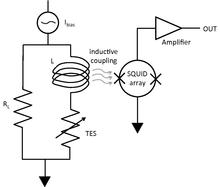
The thermal runaway problem was solved in 1995 by K. D. Irwin by voltage-biasing the TES, establishing stable negative electrothermal feedback, and coupling them to superconducting quantum interference devices (SQUID) current amplifiers.
[4] At higher energies, the primary obstacle to absorption is transmission, not reflection, and thus an absorber with high photon stopping power and low heat capacity is desirable; a bismuth film is often employed.
[5] The output signal is proportional to the temperature change of the absorber, and thus for maximal sensitivity, a TES should have low heat capacity and a narrow transition.
[6] Bilayer and multilayer TESs are another popular fabrication approach, where thin films of different materials are combined to achieve the desired Tc.
[3][4] Other devices use mechanical means of controlling the thermal conductance such as building the TES on a sub-micrometre membrane over a hole in the substrate or in the middle of a sparse "spiderweb" structure.
Among their most striking attributes are an unprecedented high detection efficiency customizable to wavelengths from the millimeter regime to gamma rays[3][4] and a theoretical negligible background dark count level (less than 1 event in 1000 s from intrinsic thermal fluctuations of the device[5]).
In contrast, TES detectors must be operated in a cryogenic environment, output a signal that must be further analyzed to identify photons, and have a jitter of approximately 100 ns.