Multigate device
A multigate device employing independent gate electrodes is sometimes called a multiple-independent-gate field-effect transistor (MIGFET).
Multi-gate transistors are one of the several strategies being developed by MOS semiconductor manufacturers to create ever-smaller microprocessors and memory cells, colloquially referred to as extending Moore's law (in its narrow, specific version concerning density scaling, exclusive of its careless historical conflation with Dennard scaling).
[1] Development efforts into multigate transistors have been reported by the Electrotechnical Laboratory, Toshiba, Grenoble INP, Hitachi, IBM, TSMC, UC Berkeley, Infineon Technologies, Intel, AMD, Samsung Electronics, KAIST, Freescale Semiconductor, and others, and the ITRS predicted correctly that such devices will be the cornerstone of sub-32 nm technologies.
[2] The primary roadblock to widespread implementation is manufacturability, as both planar and non-planar designs present significant challenges, especially with respect to lithography and patterning.
Other complementary strategies for device scaling include channel strain engineering, silicon-on-insulator-based technologies, and high-κ/metal gate materials.
The wrap-around gate structure provides a better electrical control over the channel and thus helps in reducing the leakage current and overcoming other short-channel effects.
[9][10][11] In the late 1990s, Digh Hisamoto began collaborating with an international team of researchers on further developing DELTA technology, including TSMC's Chenming Hu and a UC Berkeley research team including Tsu-Jae King Liu, Jeffrey Bokor, Xuejue Huang, Leland Chang, Nick Lindert, S. Ahmed, Cyrus Tabery, Yang-Kyu Choi, Pushkar Ranade, Sriram Balasubramanian, A. Agarwal and M. Ameen.
[15] In the technical literature, FinFET is used somewhat generically to describe any fin-based, multigate transistor architecture regardless of number of gates.
[21] The next month, the rival company TSMC announced start early or "risk" production of 16 nm FinFETs in November 2013.
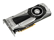
[24] The company has tried to produce a design to provide a "generational jump in power efficiency" while also offering stable frame rates for graphics, gaming, virtual reality, and multimedia applications.
They realized that the fully depleted (FD) body of a narrow bulk Si-based transistor helped improve switching due to a reduced body-bias effect.
A year later, in September 2003, AMD announced that it was working on similar technology at the International Conference on Solid State Devices and Materials.
[35] On April 23, 2012, Intel released a new line of CPUs, termed Ivy Bridge, which feature tri-gate transistors.
[38] Tri-gate fabrication was used by Intel for the non-planar transistor architecture used in Ivy Bridge, Haswell and Skylake processors.
GAAFET, also known as a surrounding-gate transistor (SGT),[44][45] is similar in concept to a FinFET except that the gate material surrounds the channel region on all sides.
[49][50][45] Masuoka, best known as the inventor of flash memory, later left Toshiba and founded Unisantis Electronics in 2004 to research surrounding-gate technology along with Tohoku University.
Multigate transistors also provide a better analog performance due to a higher intrinsic gain and lower channel length modulation.
The primary challenges to integrating nonplanar multigate devices into conventional semiconductor manufacturing processes include: BSIMCMG106.0.0,[65] officially released on March 1, 2012 by UC Berkeley BSIM Group, is the first standard model for FinFETs.
If the channel doping concentration is low enough to be neglected, computational efficiency can be further improved by a setting a specific flag (COREMOD = 1).
Volume inversion is included in the solution of Poisson's equation, hence the subsequent I–V formulation automatically captures the volume-inversion effect.
Analysis of electrostatic potential in the body of MG MOSFETs provided a model equation for short-channel effects (SCE).