Band diagram
In solid-state physics of semiconductors, a band diagram is a diagram plotting various key electron energy levels (Fermi level and nearby energy band edges) as a function of some spatial dimension, which is often denoted x.
The difference is that in a band structure plot the horizontal axis represents the wave vector of an electron in an infinitely large, homogeneous material (a crystal or vacuum), whereas in a band diagram the horizontal axis represents position in space, usually passing through multiple materials.
For this reason, the band diagram can only accurately depict evolution of band structures over long length scales, and has difficulty in showing the microscopic picture of sharp, atomic scale interfaces between different materials (or between a material and vacuum).
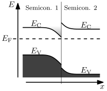
Practically all types of interface develop a charge imbalance, though for different reasons: Knowing how bands will bend when two different types of materials are brought in contact is key to understanding whether the junction will be rectifying (Schottky) or ohmic.
The degree of band bending depends on the relative Fermi levels and carrier concentrations of the materials forming the junction.