Depletion region
The only elements left in the depletion region are ionized donor or acceptor impurities.
Understanding the depletion region is key to explaining modern semiconductor electronics: diodes, bipolar junction transistors, field-effect transistors, and variable capacitance diodes all rely on depletion region phenomena.
By definition, the N-type semiconductor has an excess of free electrons (in the conduction band) compared to the P-type semiconductor, and the P-type has an excess of holes (in the valence band) compared to the N-type.
Following transfer, the diffused electrons come into contact with holes and are eliminated by recombination in the P-side.
Likewise, the diffused holes are recombined with free electrons so eliminated in the N-side.
This creates an electric field that provides a force opposing the charge diffusion.
When the electric field is sufficiently strong to cease further diffusion of holes and electrons, the depletion region reaches the equilibrium.
In the P-side of the depletion region, where holes drift by the electric field with the electrical conductivity σ and diffuse with the diffusion constant D, the net current density is given by
is the electric field, e is the elementary charge (1.6×10⁻¹⁹ coulomb), and p is the hole density (number per unit volume).
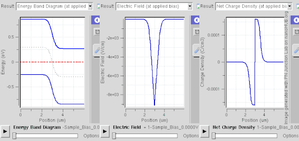
Forward bias (applying a positive voltage to the P-side with respect to the N-side) narrows the depletion region and lowers the barrier to carrier injection (shown in the figure to the right).
In more detail, majority carriers get some energy from the bias field, enabling them to go into the region and neutralize opposite charges.
The carriers can be recombined to the ions but thermal energy immediately makes recombined carriers transition back as Fermi energy is in proximity.
When bias is strong enough that the depletion region becomes very thin, the diffusion component of the current (through the junction interface) greatly increases and the drift component decreases.
In this case, the net current flows from the P-side to the N-side.
The carrier density is large (it varies exponentially with the applied bias voltage), making the junction conductive and allowing a large forward current.
[3] The mathematical description of the current is provided by the Shockley diode equation.
Essentially, majority carriers are pushed away from the junction, leaving behind more charged ions.
From a full depletion analysis as shown in figure 2, the charge would be approximated with a sudden drop at its limit points which in reality is gradual and is explained by Poisson's equation.
The final equation would then be arranged so that the function of depletion layer width
They leave behind a depleted region that is insulating because no mobile holes remain; only the immobile, negatively charged acceptor impurities.
The greater the positive charge placed on the gate, the more positive the applied gate voltage, and the more holes that leave the semiconductor surface, enlarging the depletion region.
The above discussion applies for positive voltages low enough that an inversion layer does not form.)
If the gate material is polysilicon of opposite type to the bulk semiconductor, then a spontaneous depletion region forms if the gate is electrically shorted to the substrate, in much the same manner as described for the p–n junction above.
are the number of ionized donors and acceptors "per unit of length", respectively.
The electric field is zero outside of the depletion width (seen in above figure) and therefore Gauss's law implies that the charge density in each region balance – as shown by the first equation in this sub-section.
[6] A more complete analysis would take into account that there are still some carriers near the edges of the depletion region.
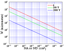
acceptors per unit volume, then charge neutrality requires the depletion width w to satisfy the relationship: If the depletion width becomes wide enough, then electrons appear in a very thin layer at the semiconductor-oxide interface, called an inversion layer because they are oppositely charged to the holes that prevail in a P-type material.
When an inversion layer forms, the depletion width ceases to expand with increase in gate charge Q.
In this case, neutrality is achieved by attracting more electrons into the inversion layer.
This effect occurs because the electric field in the depletion layer varies linearly in space from its (maximum) value