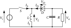
Buck–boost converter
In the inverting topology, the output voltage is of the opposite polarity than the input.
The output voltage is adjustable based on the duty cycle of the switching transistor.
One possible drawback of this converter is that the switch does not have a terminal at ground; this complicates the driving circuitry.
Also during this time, the inductor will store energy in the form of a magnetic field.
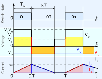
If the current through the inductor L never falls to zero during a commutation cycle, the converter is said to operate in continuous mode.
During the Off-state, the switch S is open, so the inductor current flows through the load.
If we assume zero voltage drop in the diode, and a capacitor large enough for its voltage to remain constant, the evolution of IL is: Therefore, the variation of IL during the Off-period is: As we consider that the converter operates in steady-state conditions, the amount of energy stored in each of its components has to be the same at the beginning and at the end of a commutation cycle.
by their expressions yields: This can be written as: This in return yields that: From the above expression it can be seen that the polarity of the output voltage is always negative (because the duty cycle goes from 0 to 1), and that its absolute value increases with D, theoretically up to minus infinity when D approaches 1.
In some cases, the amount of energy required by the load is small enough to be transferred in a time smaller than the whole commutation period.
The only difference in the principle described above is that the inductor is completely discharged at the end of the commutation cycle (see waveforms in figure 4).
Although slight, the difference has a strong effect on the output voltage equation.
) is During the off-period, IL falls to zero after δ.T: Using the two previous equations, δ is: The load current
As told at the beginning of this section, the converter operates in discontinuous mode when low current is drawn by the load, and in continuous mode at higher load current levels.
The limit between discontinuous and continuous modes is reached when the inductor current falls to zero exactly at the end of the commutation cycle.
(output current at the limit between continuous and discontinuous modes) is given by: Replacing
A two-switch buck-boost converter can be built with two diodes, but upgrading the diodes to FET switches doesn't cost much extra while efficiency improves due to the lower voltage drop.
That means that the power is transmitted without losses from the input voltage source to the load.
Therefore, a fraction of the power managed by the converter is dissipated by these parasitic resistances.
This assumption is acceptable because an inductor is made of one long wound piece of wire, so it is likely to exhibit a non-negligible parasitic resistance (RL).
are respectively the average voltage across the inductor and the switch over the commutation cycle.
If we consider that the converter operates in steady-state, the average current through the inductor is constant.
When it is off, the diode is forward biased (we consider the continuous mode operation), therefore
But when RL increases, the voltage gain of the converter decreases compared to the ideal case.