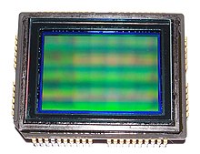
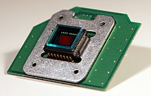
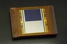
Charge-coupled device
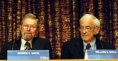
[2][4] In the late 1960s, Willard Boyle and George E. Smith at Bell Labs were researching MOS technology while working on semiconductor bubble memory.
As it was fairly straightforward to fabricate a series of MOS capacitors in a row, they connected a suitable voltage to them so that the charge could be stepped along from one to the next.
The first experimental device demonstrating the principle was a row of closely spaced metal squares on an oxidized silicon surface electrically accessed by wire bonds.
[9] The first working CCD made with integrated circuit technology was a simple 8-bit shift register, reported by Tompsett, Amelio and Smith in August 1970.
[11] Several companies, including Fairchild Semiconductor, RCA and Texas Instruments, picked up on the invention and began development programs.
[12] Steven Sasson, an electrical engineer working for the Kodak Apparatus Division, invented a digital still camera using this same Fairchild 100 × 100 CCD in 1975.
[13] The interline transfer (ILT) CCD device was proposed by L. Walsh and R. Dyck at Fairchild in 1973 to reduce smear and eliminate a mechanical shutter.
To further reduce smear from bright light sources, the frame-interline-transfer (FIT) CCD architecture was developed by K. Horii, T. Kuroda and T. Kunii at Matsushita (now Panasonic) in 1981.
[2] The first KH-11 KENNEN reconnaissance satellite equipped with charge-coupled device array (800 × 800 pixels)[citation needed] technology for imaging was launched in December 1976.
[14] Under the leadership of Kazuo Iwama, Sony started a large development effort on CCDs involving a significant investment.
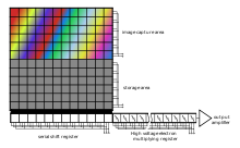
Once the array has been exposed to the image, a control circuit causes each capacitor to transfer its contents to its neighbor (operating as a shift register).
However, it takes time to reach this thermal equilibrium: up to hours in high-end scientific cameras cooled at low temperature.
[22] Initially after biasing, the holes are pushed far into the substrate, and no mobile electrons are at or near the surface; the CCD thus operates in a non-equilibrium state called deep depletion.
Simon Sze details the advantages of a buried-channel device:[23] This thin layer (= 0.2–0.3 micron) is fully depleted and the accumulated photogenerated charge is kept away from the surface.
The clocking of the gates, alternately high and low, will forward and reverse bias the diode that is provided by the buried channel (n-doped) and the epitaxial layer (p-doped).
The peristaltic CCD has an additional implant that keeps the charge away from the silicon/silicon dioxide interface and generates a large lateral electric field from one gate to the next.
The downside to the frame-transfer architecture is that it requires twice the silicon real estate of an equivalent full-frame device; hence, it costs roughly twice as much.
The advantage is not free, however, as the imaging area is now covered by opaque strips dropping the fill factor to approximately 50 percent and the effective quantum efficiency by an equivalent amount.
Modern designs have addressed this deleterious characteristic by adding microlenses on the surface of the device to direct light away from the opaque regions and on the active area.
On the other hand, for those applications that require the best possible light collection and issues of money, power and time are less important, the full-frame device is the right choice.
Cooling reduces the array's dark current, improving the sensitivity of the CCD to low light intensities, even for ultraviolet and visible wavelengths.
Professional observatories often cool their detectors with liquid nitrogen to reduce the dark current, and therefore the thermal noise, to negligible levels.
The disadvantage of such a CCD is the higher cost: the cell area is basically doubled, and more complex control electronics are needed.
The phosphor screen finally converts the multiplied electrons back to photons which are guided to the CCD by a fiber optic or a lens.
To avoid multiple counts in one pixel due to coincident photons in this mode of operation, high frame rates are essential.
However, high-end EMCCD cameras are equipped with a permanent hermetic vacuum system confining the chip to avoid condensation issues.
More recently, these types of CCDs have broken into the field of biomedical research in low-light applications including small animal imaging, single-molecule imaging, Raman spectroscopy, super resolution microscopy as well as a wide variety of modern fluorescence microscopy techniques thanks to greater SNR in low-light conditions in comparison with traditional CCDs and ICCDs.
[31] CCD cameras used in astrophotography often require sturdy mounts to cope with vibrations from wind and other sources, along with the tremendous weight of most imaging platforms.
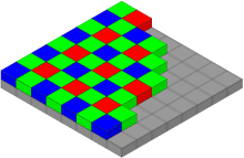
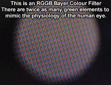
Better color separation can be reached by three-CCD devices (3CCD) and a dichroic beam splitter prism, that splits the image into red, green and blue components.
Between acquisitions, the sensor is moved in pixel dimensions, so that each point in the visual field is acquired consecutively by elements of the mask that are sensitive to the red, green, and blue components of its color.