CPU multiplier
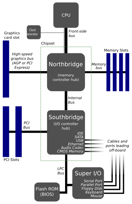
The external address and data buses of the CPU (often collectively termed front side bus (FSB) in PC contexts) also use the external clock as a fundamental timing base; however, they could also employ a (small) multiple of this base frequency (typically two or four) to transfer data faster.
To determine the actual bus frequency for processors that use dual-data rate (DDR) buses (AMD Athlon and Duron) and quad-data rate buses (all Intel microprocessors starting from Pentium 4) the effective bus speed should be divided by 2 for AMD or 4 for Intel.
Nearly every desktop CPU produced since the introduction of the 486DX2 in 1992 has employed a clock multiplier to run its internal logic at a higher frequency than its external bus, but still remain synchronous with it.
This improves the CPU performance by relying on internal cache memories or wide buses (often also capable of more than one transfer per clock cycle) to make up for the frequency difference.
These adjustments provide the two common methods of overclocking and underclocking a computer, perhaps combined with some adjustment of CPU or memory voltages (changing oscillator crystals occurs only rarely); note that careless overclocking can cause damage to a CPU or other component due to overheating or even voltage breakdown.
[citation needed] By the late 1990s almost all high-performance processors (excluding typical embedded systems) run at higher speeds than their external buses, so the term "clock doubling" has lost much of its impact.
For CPU-bound applications, clock doubling will theoretically improve the overall performance of the machine substantially, provided the fetching of data from memory does not prove a bottleneck.