CSG 65CE02
[1] It is a member of the MOS Technology 6502 family, developed from the CMOS WDC 65C02 released by the Western Design Center in 1983.
Around 1981, the main licensees of the 6502 design, Rockwell Semiconductor, GTE and Signetics, began a redesign effort with Mensch that led to the WDC 65C02.
This was mainly a CMOS implementation of the original NMOS 6502 that used 10 to 20 times less power, but it also included a number of new instructions to help improve the code density in certain applications.
New instructions included INA/DEA to increment and decrement the accumulator, STZ to write a zero to a memory location, and BRA which was a jump with a branch-style 1-byte relative address.
For both of these reasons, the ability to handle "large" amounts of memory was not required, and many processors had operating modes that worked with small portions of a larger address space in order to offer higher performance.
By the 1980s, these assumptions were no longer valid; many machines based on these processors now shipped with the maximum 64 kB that the 6502 could address, using the far less expensive and denser dynamic RAM.
The speed advantages of the zero page addressing mode remained, but now existing within a memory space that was dramatically larger.
[1] It is fabricated using 2 µm CMOS technology, allowing for lower power operation compared to previous NMOS and HMOS versions of the 65xx family.
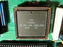
[3] The 4510 is a system in package (SiP) variant of the 65CE02 that includes two 6526 CIA I/O port controllers and a custom MMU to expand the address space to 20 bit (1 megabyte).