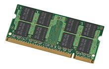
DDR2 SDRAM
The two factors combine to produce a total of four data transfers per internal clock cycle.
Alternatively, DDR2 memory operating at twice the external data bus clock rate as DDR may provide twice the bandwidth with the same latency.
Both performed worse than the original DDR specification due to higher latency, which made total access times longer.
DDR2 started to become competitive against the older DDR standard by the end of 2004, as modules with lower latencies became available.
DDR2's bus frequency is boosted by electrical interface improvements, on-die termination, prefetch buffers and off-chip drivers.
Power savings are achieved primarily due to an improved manufacturing process through die shrinkage, resulting in a drop in operating voltage (1.8 V compared to DDR's 2.5 V).
The lower memory clock frequency may also enable power reductions in applications that do not require the highest available data rates.
In addition, JEDEC states that memory modules must withstand up to 2.3 volts before incurring permanent damage (although they may not actually function correctly at that level).
At least one manufacturer has reported this reflects successful testing at a higher-than-standard data rate[9] whilst others simply round up for the name.
ATI has since designed the GDDR technology further into GDDR3, which is based on DDR2 SDRAM, though with several additions suited for graphics cards.
These chips cannot achieve the clock rates of GDDR3 but are inexpensive and fast enough to be used as memory on mid-range cards.
Note**: JEDEC website requires registration ($2,500 membership) for viewing or downloading of these documents: http://www.jedec.org/standards-documents