Delta-sigma modulation
Delta-sigma (ΔΣ; or sigma-delta, ΣΔ) modulation is an oversampling method for encoding signals into low bit depth digital signals at a very high sample-frequency as part of the process of delta-sigma analog-to-digital converters (ADCs) and digital-to-analog converters (DACs).
In both cases, the temporary use of a low bit depth signal at a higher sampling frequency simplifies circuit design and takes advantage of the efficiency and high accuracy in time of digital electronics.
Primarily because of its cost efficiency and reduced circuit complexity, this technique has found increasing use in modern electronic components such as DACs, ADCs, frequency synthesizers, switched-mode power supplies and motor controllers.
Such higher-bit methods seek accuracy in amplitude directly, but require extremely precise components and so may suffer from poor linearity.
The differentiation alters the signal's spectrum by amplifying high-frequency noise, attenuating low-frequencies,[2] and dropping the DC component.
Since the accumulated error signal is lowpass filtered by the delta-sigma modulator's integrator before being quantized, the subsequent negative feedback of its quantized result effectively subtracts the low frequency components of the quantization noise while leaving the higher frequency components of the noise.
The seminal[4] paper combining feedback with oversampling to achieve delta modulation was by F. de Jager of Philips Research Laboratories in 1952.
[6] It was not named as such until a 1962 paper[7] by Inose et al. of University of Tokyo, which came up with the idea of adding a filter in the forward path of the delta modulator.
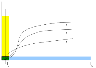
Some avenues of variation (which may be applied in different combinations) are the modulator's order, the quantizer's bitdepth, the manner of decimation, and the oversampling ratio.
One criticism of 1-bit quantization is that adequate amounts of dither cannot be used in the feedback loop, so distortion can be heard under some conditions (more discussion at Direct Stream Digital § DSD vs.
The proposal to decimate oversampled delta-sigma data using digital filtering before converting it into PCM audio was made by D. J. Goodman at Bell Labs in 1969,[15] to reduce the ΔΣ signal from its high sampling rate while increasing its bit depth.
ΔΣ ADCs reduce the amount of this noise in the baseband by spreading it out and shaping it so it is mostly in higher frequencies.
so the system effectively acts as a high-pass filter on the noise that starts at 0 at DC, then gradually rises until it reaches the cutoff frequency, and then levels off.
Note: many sources[11]§6.1[26][27] also analyze a ΔΣ ADC's modulation loop in the z-domain, which implicitly treats the continuous analog input as a discrete-time signal.
This may be a valid approximation provided that the input signal is already bandlimited and can be assumed to be not changing on time scales higher than the sampling rate.
In practice, circuits inevitably experience other noise sources that limit resolution, making the higher-resolution cells impractical.
The net effect is a simpler implementation that has the profound added benefit of shaping the quantization noise to be mostly in frequencies above the signals of interest.
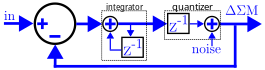
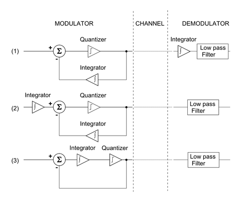
It is functionally the same Analog-to-Digital ΔΣ modulation loop in Figure 1 (note: the 2-input inverting integrator combines the summing junction and integrator and produces a negative feedback result, and the flip-flop combines the sampled quantizer and conveniently naturally functions as a 1-bit DAC too).
This circuit can be laid out on a breadboard with inexpensive discrete components (note some variations use different biasing and use simpler RC low-pass filters for integration instead of op amps).
[29][30] For simplicity, the D flip-flop is powered by dual supply voltages of VDD = +1 V and VSS = -1 V, so its binary output Q(t) is either +1 V or -1 V. The 2-input inverting op amp integrator combines s(t) with Q(t) to produce Ɛ(t):
The Greek letter epsilon is used because Ɛ(t) contains the accumulated error that is repeatedly corrected by the feedback mechanism.
Whenever a sampling event occurs: Q(t) is sent out as the resulting PDM output and also fed back to the 2-input inverting integrator.
The rightmost integrator performs digital-to-analog conversion on Q(t) to produce a demodulated analog output r(t), which reconstructs the original sine wave input as piece-wise linear diagonal segments.
It is worth noting that if no decimation ever took place, the digital representation from a 1-bit delta-sigma modulator is simply a PDM signal, which can easily be converted to analog using a low-pass filter, as simple as a resistor and capacitor.
It is often desirable to remove these higher-frequency images prior to the performing the actual delta-sigma modulation stage, in order to ease requirements on the eventual analog low-pass filter.
This can be done by upsampling using an interpolation filter and is often the first step prior to performing delta-sigma modulation in DACs.
Besides its noise shaping function, it has two more attractive properties: The technique was first presented in the early 1960s by professor Yasuhiko Yasuda while he was a student at the University of Tokyo.
[32][11] The name delta-sigma comes directly from the presence of a delta modulator and an integrator, as firstly introduced by Inose et al. in their patent[clarification needed] application.
[7] That is, the name comes from integrating or summing differences, which, in mathematics, are operations usually associated with Greek letters sigma and delta respectively.
In the 1970s, Bell Labs engineers used the terms sigma-delta because the precedent was to name variations on delta modulation with adjectives preceding delta, and an Analog Devices magazine editor justified in 1990 that the functional hierarchy is sigma-delta, because it computes the integral of a difference.