Semiconductor device fabrication
It is a multiple-step photolithographic and physico-chemical process (with steps such as thermal oxidation, thin-film deposition, ion-implantation, etching) during which electronic circuits are gradually created on a wafer, typically made of pure single-crystal semiconducting material.
[4] Within fabrication plants, the wafers are transported inside special sealed plastic boxes called FOUPs.
Additionally many machines also handle wafers in clean nitrogen or vacuum environments to reduce contamination and improve process control.
[10][11] Companies that manufacture machines used in the industrial semiconductor fabrication process include ASML, Applied Materials, Tokyo Electron and Lam Research.
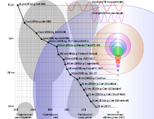
Feature size is determined by the width of the smallest lines that can be patterned in a semiconductor fabrication process, this measurement is known as the linewidth.
[34] An improved type of MOSFET technology, CMOS, was developed by Chih-Tang Sah and Frank Wanlass at Fairchild Semiconductor in 1963.
[38] In 1963, Harold M. Manasevit was the first to document epitaxial growth of silicon on sapphire while working at the Autonetics division of North American Aviation (now Boeing).
[40] Semiconductor device manufacturing has since spread from Texas and California in the 1960s to the rest of the world, including Asia, Europe, and the Middle East.
[47] In 1985, SGS (now STmicroelectronics) invented BCD, also called BCDMOS, a semiconductor manufacturing process using bipolar, CMOS and DMOS devices.
[48] Applied Materials developed the first practical multi chamber, or cluster wafer processing tool, the Precision 5000.
[68] In 1998, Applied Materials introduced the Producer, a cluster tool that had chambers grouped in pairs for processing wafers, which shared common vacuum and supply lines but were otherwise isolated, which was revolutionary at the time as it offered higher productivity than other cluster tools without sacrificing quality, due to the isolated chamber design.
When feature widths were far greater than about 10 micrometres, semiconductor purity was not as big of an issue as it is today in device manufacturing.
Today, fabrication plants are pressurized with filtered air to remove even the smallest particles, which could come to rest on the wafers and contribute to defects.
The workers in a semiconductor fabrication facility are required to wear cleanroom suits to protect the devices from contamination by humans.
[11][8] FOUPs and SMIF pods isolate the wafers from the air in the cleanroom, increasing yield because they reduce the number of defects caused by dust particles.
[140][139][141] A typical wafer is made out of extremely pure silicon that is grown into mono-crystalline cylindrical ingots (boules) up to 300 mm (slightly less than 12 inches) in diameter using the Czochralski process.
[142] In semiconductor device fabrication, the various processing steps fall into four general categories: deposition, removal, patterning, and modification of electrical properties.
Modification of electrical properties now also extends to the reduction of a material's dielectric constant in low-κ insulators via exposure to ultraviolet light in UV processing (UVP).
Many pieces of equipment handle wafers between these chambers in an internal nitrogen or vacuum environment to improve process control.
Gate-first consists of depositing the high-k dielectric and then the gate metal such as Tantalum nitride whose workfunction depends on whether the transistor is NMOS or PMOS, polysilicon deposition, gate line patterning, source and drain ion implantation, dopant anneal, and silicidation of the polysilicon and the source and drain.
In production, plasma ALE is commonly used, which removes materials unidirectionally, creating structures with vertical walls.
Thermal ALE can also be used to remove materials isotropically, in all directions at the same time but without the capability to create vertical walls.
The various metal layers are interconnected by etching holes (called "vias") in the insulating material and then depositing tungsten in them with a CVD technique using tungsten hexafluoride; this approach can still be (and often is) used in the fabrication of many memory chips such as dynamic random-access memory (DRAM), because the number of interconnect levels can be small (no more than four).
As the number of interconnect levels increases, planarization of the previous layers is required to ensure a flat surface prior to subsequent lithography.
Virtual metrology has been used to predict wafer properties based on statistical methods without performing the physical measurement itself.
[1] Once the front-end process has been completed, the semiconductor devices or chips are subjected to a variety of electrical tests to determine if they function properly.
Currently, electronic dye marking is possible if wafer test data (results) are logged into a central computer database and chips are "binned" (i.e. sorted into virtual bins) according to predetermined test limits such as maximum operating frequencies/clocks, number of working (fully functional) cores per chip, etc.
The resulting binning data can be graphed, or logged, on a wafer map to trace manufacturing defects and mark bad chips.
Automation and the use of mini environments inside of production equipment, FOUPs and SMIFs have enabled a reduction in defects caused by dust particles.
Most fabrication facilities employ exhaust management systems, such as wet scrubbers, combustors, heated absorber cartridges, etc.,[198][199][200] to control the risk to workers and to the environment.