Standard cell
Designers use additional CAD programs such as SPICE to simulate the electronic behavior of the netlist, by declaring input stimulus (voltage or current waveforms) and then calculating the circuit's time domain (analog) response.
The simulations verify whether the netlist implements the desired function and predict other pertinent parameters, such as power consumption or signal propagation delay.
Since the logical and netlist views are only useful for abstract (algebraic) simulation, and not device fabrication, the physical representation of the standard cell must be designed too.
[2] The PEX-netlist may then be simulated again (since it contains parasitic properties) to achieve more accurate timing, power, and noise models.
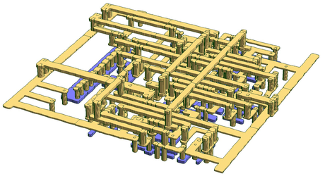
Finally, powerful place and route (PNR) tools may be used to pull everything together and synthesize (generate) Very Large Scale Integration (VLSI) layouts, in an automated fashion, from higher level design netlists and floor-plans.
Consequently, integrated circuit layout is a highly labor-intensive job, despite the existence of design tools to aid this process.
A standard-cell library is a collection of low-level electronic logic functions such as AND, OR, INVERT, flip-flops, latches, and buffers.
The key aspect with these libraries is that they are of a fixed height, which enables them to be placed in rows, easing the process of automated digital layout.
Indirectly, it also gives the designer greater freedom to perform implementation trade-offs (area vs. speed vs. power consumption).
Proper synthesis techniques ensure mathematical equivalency between the synthesized netlist and original RTL description.
The high-level synthesis tool performs the process of transforming the C-level models (SystemC, ANSI C/C++) description into a technology-dependent netlist.
Typically the standard cells have a constant size in at least one dimension that allows them to be lined up in rows on the integrated circuit.
design rule check (DRC) and layout versus schematic (LVS) are verification processes.
[2] Reliable device fabrication at modern deep-submicrometer (0.13 μm and below) requires strict observance of transistor spacing, metal layer thickness, and power density rules.
The three techniques, however, differ substantially in the details of the SPR flow (Synthesize, Place-and-Route) and physical implementation.
For digital standard-cell designs, for instance in CMOS, a common technology-independent metric for complexity measure is gate equivalents (GE).