JTAG
JTAG implements standards for on-chip instrumentation in electronic design automation (EDA) as a complementary tool to digital simulation.
The JTAG standards have been extended by multiple semiconductor chip manufacturers with specialized variants to provide vendor-specific features.
The Joint Test Action Group (JTAG) was formed in 1985 to provide a pins-out view from one IC pad to another so these faults could be discovered.
1149.1 has introduced a vast set of optional features, associated extensions to BSDL, and a new procedural description language (PDL) based on Tcl.
Today JTAG is used as the primary means of accessing sub-blocks of integrated circuits, making it an essential mechanism for debugging embedded systems which might not have any other debug-capable communications channel.
[citation needed] On most systems, JTAG-based debugging is available from the very first instruction after CPU reset, letting it assist with development of early boot software which runs before anything is set up.
Some modern debug architectures provide internal and external bus master access without needing to halt and take over a CPU.
JTAG boundary scan technology provides access to a number of logic signals of a complex integrated circuit, including the device pins.
When combined with built-in self-test (BIST), the JTAG scan chain enables a low overhead, embedded solution to test an IC for certain static faults (shorts, opens, and logic errors).
The scan chain mechanism does not generally help diagnose or test for timing, temperature or other dynamic operational errors that may occur.
The maximum operating frequency of TCK varies depending on all chips in the chain (the lowest speed must be used), but it is typically 10-100 MHz (100-10 ns per bit).
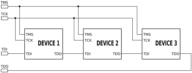
The host communicates with the TAPs by manipulating TMS and TDI in conjunction with TCK and reading results through TDO (which is the only standard host-side input).
Some layers built on top of JTAG monitor the state transitions and use uncommon paths to trigger higher-level operations.
The path creates a virtual access capability that circumvents the normal inputs and outputs, providing direct control of the device and detailed visibility for signals.
[10] The contents of the boundary scan register, including signal I/O capabilities, are usually described by the manufacturer using a part-specific BSDL file.
Examples of such chips include: Those processors are both intended for use in wireless handsets such as cell phones, which is part of the reason they include TAP controllers which modify the JTAG scan chain: Debugging low power operation requires accessing chips when they are largely powered off, and thus when not all TAPs are operational.
Non-ARM systems generally have similar capabilities, perhaps implemented using the Nexus protocols on top of JTAG, or other vendor-specific schemes.
When interesting program events approach, a person may want to single step instructions (or lines of source code) to watch how a particular misbehavior happens.
So for example a JTAG host might HALT the core, entering debug mode, and then read CPU registers using ITR and DCC.
For example, a processor used to control a motor (perhaps one driving a saw blade) may not be able to safely enter halt mode; it may need to continue handling interrupts to ensure physical safety of people and/or machinery.
In those cases, breakpoints and watchpoints trigger a special kind of hardware exception, transferring control to a debug monitor running as part of the system software.
There is a wide range of such hardware, optimized for purposes such as production testing, debugging high-speed systems, low cost microcontroller development, and so on.
For example, a microcontroller, FPGA, and ARM application processor rarely share tools, so a development board using all of those components might have three or more headers.
Production boards may omit the headers, or when space is limited may provide JTAG signal access using test points.
Some common pinouts[20] for 2.54 mm (0.100 in) pin headers are: Those connectors tend to include more than just the four standardized signals (TMS, TCK, TDI, TDO).
Other event input or output signals may be provided, or general purpose I/O (GPIO) lines, to support more complex debugging architectures.
Since modern PCs tend to omit serial ports, such integrated debug links can significantly reduce clutter for developers.)
The smart adapters eliminate link latencies for operation sequences that may involve polling for status changes between steps, and may accordingly offer higher throughput.
They generally involve either slower bit banging than a parallel port, or a microcontroller translating some command protocol to JTAG operations.
On JTAG devices with SWD capability, the TMS and TCK are used as SWDIO and SWCLK signals, providing for dual-mode programmers.