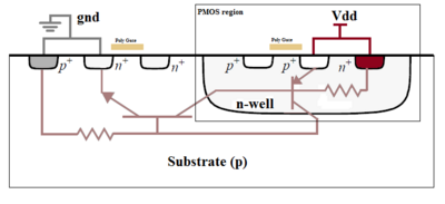
Latch-up
More specifically, it is the inadvertent creation of a low-impedance path between the power supply rails of a MOSFET circuit, triggering a parasitic structure which disrupts proper functioning of the part, possibly even leading to its destruction due to overcurrent.
The SCR parasitic structure is formed as a part of the totem-pole PMOS and NMOS transistor pair on the output drivers of the gates.
Another common cause of latch-ups is ionizing radiation which makes this a significant issue in electronic products designed for space (or very high-altitude) applications.
In CMOS processes, these transistors can create problems when the combination of n-well/p-well and substrate results in the formation of parasitic n-p-n-p structures.
Triggering these thyristor-like devices leads to a shorting of the Vdd and GND lines, usually resulting in destruction of the chip, or a system failure that can only be resolved by power-down.
[10] It is possible to design chips to be resistant to latch-up by adding a layer of insulating oxide (called a trench) that surrounds both the NMOS and the PMOS transistors.
But this will increase the size of the device so fabs give a minimum space to put a tap, for example, 10 μm in 130 nm technology.