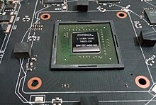
Maxwell (microarchitecture)
Maxwell introduced an improved Streaming Multiprocessor (SM) design that increased power efficiency,[1] the sixth and seventh generation PureVideo HD, and CUDA Compute Capability 5.2.
These new chips introduced few consumer-facing additional features, as Nvidia instead focused more on increasing GPU power efficiency.
The L2 cache was increased from 256 KiB on Kepler to 2 MiB on Maxwell, reducing the need for more memory bandwidth.
[2] The "SMX" streaming multiprocessor design from Kepler was also retooled and partitioned, being renamed "SMM" for Maxwell.
Dynamic Parallelism and HyperQ, two features in GK110/GK208 GPUs, are also supported across the entire Maxwell product line.
[5] Since first generation Maxwell, UEFI Graphics Output Protocol is fully supported on NVIDIA GPUs.
Second generation Maxwell GPUs introduced several new technologies: Dynamic Super Resolution,[6] Third Generation Delta Color Compression,[7] Multi-Pixel Programming Sampling,[8] Nvidia VXGI (Real-Time-Voxel-Global Illumination),[9] VR Direct,[9][10][11] Multi-Projection Acceleration,[7] Multi-Frame Sampled Anti-Aliasing(MFAA)[12] (however, support for Coverage-Sampling Anti-Aliasing(CSAA) was removed),[13] and Direct3D12 API at Feature Level 12_1.
[16] However, some of the ROPs are generally idle in the GTX 970 because there are not enough enabled SMMs to give them work to do, reducing its maximum fill rate.
[20] This comes at the cost of dividing the memory bus into high speed and low speed segments that cannot be accessed at the same time for reads, because the L2/ROP unit managing both of the GDDR5 controllers shares the read return channel and the write data bus between the GDDR5 controllers.
The theoretical double-precision processing power of a Maxwell GPU is 1/32 of the single precision performance (which has been noted as being very low compared to the previous generation Kepler).