Nanolaser
These tiny lasers can be modulated quickly and, combined with their small footprint, this makes them ideal candidates for on-chip optical computing.
Since people noticed that light has different interactions with matter at the nanoscale in the 1990s, significant progress has been made to achieve the miniaturization of lasers and increase power conversion efficiency.
[16] To approach or decrease the diffraction limit of light, one way is to improve the reflectivity of gain medium, such as using photonic bandgap and nanowires.
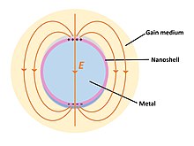
Another effective way to exceed the diffraction limit is to convert light into surface plasmons in nanostructuralized metals, for amplification in cavity.
[14][17] Recently, new mechanisms of strong light confinement for nanolasers including parity–time symmetry,[18] photonic topological insulators,[19][20] and bound states in the continuum[21] have been proposed.
The biggest advantages of nanolasers are their ultra-small physical volumes to improve energy efficiencies, decrease lasing thresholds, and achieve high modulation speeds.
When there is a defect in the periodic structure, the two-dimensional or three-dimensional photonic crystal structure will confine the light in the space of the diffractive limit and produce the Fano resonance phenomenon, which means a high quality factor with a strong light confinement for lasers.
The width of nanowires is large enough to ignore the quantum size effect, but they are high quality one-dimensional waveguides with cylindrical, rectangular, trigonal, and hexagonal cross-sections.
The attraction between electrons and ions allows for the oscillation of electrode cloud and the formation of local surface from polarization excimer.
When the gain–loss contrast and coupling constant between two identical, closely located cavities are controlled, the phase transition of lasing modes occurs at an exceptional point.
[39] Nanowire nanolasers can be capable of optical detection at the scale of a single molecule with high resolution and ultrafast modulation.
[40][41] Plasmonic nanolaser sensors have recently been demonstrated that can detect specific molecules in air and be used for optical biosensors.
[23][43] For nanolasers, the realization of electrically injected or pumped operation at room temperature is a key step towards its practical application.
Moreover, it still remains a challenge to realize cavity configuration engineering and metal quality improvement, which are crucial to satisfy the high-performance requirement of nanolasers and achieve their applications.
[44] Recently, nanolaser arrays show great potential to increase the power efficiency and accelerate modulation speed.


