Organic electronics
[1][2][3] Attractive properties of polymeric conductors include their electrical conductivity (which can be varied by the concentrations of dopants) and comparatively high mechanical flexibility.
Challenges to the implementation of organic electronic materials are their inferior thermal stability, high cost, and diverse fabrication issues.
Lilienfeld[6] first proposed the field-effect transistor in 1930, but the first OFET was not reported until 1987, when Koezuka et al. constructed one using Polythiophene[7] which shows extremely high conductivity.
Other conductive polymers have been shown to act as semiconductors, and newly synthesized and characterized compounds are reported weekly in prominent research journals.
Specifically, the organic compound pyrene was shown to form semiconducting charge-transfer complex salts with halogens.
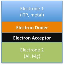
The OLED device incorporated a double-layer structure motif composed of copper phthalocyanine and a derivative of perylenetetracarboxylic dianhydride.
Both organic synthesis and advanced dispersion techniques can be used to tune the electrical properties of conductive polymers, unlike typical inorganic conductors.
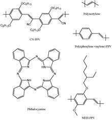
Small molecule OLEDs (SM-OLEDs) include tris(8-hydroxyquinolinato)aluminium[17] fluorescent and phosphorescent dyes, and conjugated dendrimers.
While this method enables the formation of well-controlled homogeneous film; is hampered by high cost and limited scalability.
A field-effect transistor (FET) is any semiconductor material that utilizes electric field to control the shape of a channel of one type of charge carrier, thereby changing its conductivity.
Due to its low solubility in most organic solvents, it's difficult to fabricate thin film transistors (TFTs) from pentacene itself using conventional spin-cast or, dip coating methods, but this obstacle can be overcome by using the derivative TIPS-pentacene.
Protomorphous solar cells prove to be a promising concept for efficient and low-cost photovoltaics on cheap and flexible substrates for large-area production as well as small and mobile applications.
One ink must not damage another, and low temperature annealing is vital if low-cost flexible materials such as paper and plastic film are to be used.
There is much sophisticated engineering and chemistry involved here, with iTi, Pixdro, Asahi Kasei, Merck & Co.|Merck, BASF, HC Starck, Sunew, Hitachi Chemical, and Frontier Carbon Corporation among the leaders.
Both solution processing and vacuum based methods produce amorphous and polycrystalline films with variable degree of disorder.
"Wet" coating techniques require polymers to be dissolved in a volatile solvent, filtered and deposited onto a substrate.
The doctor-blade technique results in a minimal material loss and was primarily developed for large area thin film production.
However, all three of these types of solar cells share the approach of sandwiching the organic electronic layer between two metallic conductors, typically indium tin oxide.
There are mainly two types of organic field-effect transistor, based on the semiconducting layer's charge transport, namely p-type (such as dinaphtho[2,3-b:2′,3′-f]thieno[3,2-b]thiophene, DNTT),[36] and n-type (such phenyl C61 butyric acid methyl ester, PCBM).