Photomultiplier tube
The combination of high gain, low noise, high frequency response or, equivalently, ultra-fast response, and large area of collection has maintained photomultipliers an essential place in low light level spectroscopy, confocal microscopy, Raman spectroscopy, fluorescence spectroscopy, nuclear and particle physics, astronomy, medical diagnostics including blood tests, medical imaging, motion picture film scanning (telecine), radar jamming, and high-end image scanners known as drum scanners.
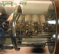
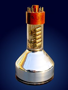
Photomultipliers are typically constructed with an evacuated glass housing (using an extremely tight and durable glass-to-metal seal like other vacuum tubes), containing a photocathode, several dynodes, and an anode.
Incident photons strike the photocathode material, which is usually a thin vapor-deposited conducting layer on the inside of the entry window of the device.
This large number of electrons reaching the anode results in a sharp current pulse that is easily detectable, for example on an oscilloscope, signaling the arrival of the photon(s) at the photocathode ≈50 nanoseconds earlier.
There are two common photomultiplier orientations, the head-on or end-on (transmission mode) design, as shown above, where light enters the flat, circular top of the tube and passes the photocathode, and the side-on design (reflection mode), where light enters at a particular spot on the side of the tube, and impacts on an opaque photocathode.
The invention of the photomultiplier is predicated upon two prior achievements, the separate discoveries of the photoelectric effect and of secondary emission.
[2] Significant for practical applications, Elster and Geitel two years later demonstrated the same effect using visible light striking alkali metals (potassium and sodium).
It is worthwhile to note that Heinrich Hertz, working 18 years earlier, had not recognized that the kinetic energy of the emitted electrons is proportional to the frequency but independent of the optical intensity.
[6] The application of the newly discovered secondary emission to the amplification of signals was only proposed after World War I by Westinghouse scientist Joseph Slepian in a 1919 patent.
Television had been pursued with primitive prototypes for decades prior to the 1934 introduction of the first practical video camera (the iconoscope).
Photomultiplier technology was pursued to enable television camera tubes, such as the iconoscope and (later) the orthicon, to be sensitive enough to be practical.
So the stage was set to combine the dual phenomena of photoemission (i.e., the photoelectric effect) with secondary emission, both of which had already been studied and adequately understood, to create a practical photomultiplier.
The first documented photomultiplier demonstration dates to the early 1934 accomplishments of an RCA group based in Harrison, NJ.
These accomplishments were finalized prior to June 1934 as detailed in the manuscript submitted to Proceedings of the Institute of Radio Engineers (Proc.
Accordingly, leading international research organizations turned their attention towards improving photomultipliers to achieve higher gain with multiple stages.
The Soviet device used a magnetic field to confine the secondary electrons and relied on the Ag-O-Cs photocathode which had been demonstrated by General Electric in the 1920s.
By October 1935, Vladimir Zworykin, George Ashmun Morton, and Louis Malter of RCA in Camden, NJ submitted their manuscript describing the first comprehensive experimental and theoretical analysis of a multiple dynode tube — the device later called a photomultiplier[13] — to Proc.
In the early 1940s, the JEDEC (Joint Electron Device Engineering Council), an industry committee on standardization, developed a system of designating spectral responses.
No suitable photoemissive surfaces have yet been reported to detect wavelengths longer than approximately 1700 nanometers, which can be approached by a special (InP/InGaAs(Cs)) photocathode.
The Lancaster, Pennsylvania facility was opened by the U.S. Navy in 1942 and operated by RCA for the manufacture of radio and microwave tubes.
Photonis USA operates the former Galileo Corporation Scientific Detector Products Group (Sturbridge, Massachusetts), which had been purchased by Burle Industries in 1999.
The group is known for microchannel plate detector (MCP) electron multipliers—an integrated micro-vacuum tube version of photomultipliers.
On 9 March 2009, Photonis announced that it would cease all production of photomultipliers at both the Lancaster, Pennsylvania and the Brive, France plants.
High dark current; used mainly in near-infrared, with the photocathode cooled; GaAs:Cs, caesium-activated gallium arsenide, flat response from 300 to 850 nm, fading towards ultraviolet and to 930 nm; InGaAs:Cs, caesium-activated indium gallium arsenide, higher infrared sensitivity than GaAs:Cs, between 900–1000 nm much higher signal-to-noise ratio than Ag-O-Cs; Sb-Cs, (also called S11) caesium-activated antimony, used for reflective mode photocathodes; response range from ultraviolet to visible, widely used; bialkali (Sb-K-Cs, Sb-Rb-Cs), caesium-activated antimony-rubidium or antimony-potassium alloy, similar to Sb:Cs, with higher sensitivity and lower noise.
can be used for transmission-mode; favorable response to a NaI:Tl scintillator flashes makes them widely used in gamma spectroscopy and radiation detection; high-temperature bialkali (Na-K-Sb), can operate up to 175 °C, used in well logging, low dark current at room temperature; multialkali (Na-K-Sb-Cs), (also called S20), wide spectral response from ultraviolet to near-infrared, special cathode processing can extend range to 930 nm, used in broadband spectrophotometers; solar-blind (Cs-Te, Cs-I), sensitive to vacuum-UV and ultraviolet, insensitive to visible light and infrared (Cs-Te has cutoff at 320 nm, Cs-I at 200 nm).
Another option is to add overcurrent protection in the external circuit, so that when the measured anode current exceeds a safe limit, the high voltage is reduced.
[23] Photomultipliers are used in research laboratories to measure the intensity and spectrum of light-emitting materials such as compound semiconductors and quantum dots.
The aforementioned refers to measurement of light fluxes that, while small, nonetheless amount to a continuous stream of multiple photons.
For smaller photon fluxes, the photomultiplier can be operated in photon-counting, or Geiger, mode (see also Single-photon avalanche diode).
Nonetheless, the ability to detect single photons striking the primary photosensitive surface itself reveals the quantization principle that Einstein put forth.