Polycrystalline silicon
The photovoltaic industry also produces upgraded metallurgical-grade silicon (UMG-Si), using metallurgical instead of chemical purification processes.
[1] When produced for the electronics industry, polysilicon contains impurity levels of less than one part per billion (ppb), while polycrystalline solar grade silicon (SoG-Si) is generally less pure.
[2] The polysilicon feedstock – large rods, usually broken into chunks of specific sizes and packaged in clean rooms before shipment – is directly cast into multicrystalline ingots or submitted to a recrystallization process to grow single crystal boules.
The boules are then sliced into thin silicon wafers and used for the production of solar cells, integrated circuits and other semiconductor devices.
Polysilicon consists of small crystals, also known as crystallites, giving the material its typical metal flake effect.
At the component level, polysilicon has long been used as the conducting gate material in MOSFET and CMOS processing technologies.
The deposition of polycrystalline silicon on plastic substrates is motivated by the desire to be able to manufacture digital displays on flexible screens.
This allows more complex, high-speed circuitry to be created on the glass substrate along with the a-Si devices, which are still needed for their low-leakage characteristics.
A complete polysilicon active layer process is also used in some cases where a small pixel size is required, such as in projection displays.
[6] The solar industry was severely hindered by a shortage in supply of polysilicon feedstock and was forced to idle about a quarter of its cell and module manufacturing capacity in 2007.
[8] Monocrystalline silicon is higher priced and a more efficient semiconductor than polycrystalline as it has undergone additional recrystallization via the Czochralski method.
When a polysilicon deposition process becomes mass-transport-limited, the reaction rate becomes dependent primarily on reactant concentration, reactor geometry, and gas flow.
A plot of the logarithm of the deposition rate against the reciprocal of the absolute temperature in the surface-reaction-limited region results in a straight line whose slope is equal to –qEa/k.
Above 650 °C, poor deposition uniformity and excessive roughness will be encountered due to unwanted gas-phase reactions and silane depletion.
Recent investigations have shown that e-beam evaporation, followed by SPC (if needed) can be a cost-effective and faster alternative for producing solar-grade poly-Si thin films.
[13] The process converts metallurgical-grade Si, of approximately 98% purity, to SiHCl3 and then to silicon in a reactor, thus removing transition metal and dopant impurities.
[14] Upgraded metallurgical-grade (UMG) silicon (also known as UMG-Si) for solar cells is being produced as a low cost alternative to polysilicon created by the Siemens process.
UMG-Si greatly reduces impurities in a variety of ways that require less equipment and energy than the Siemens process.
It has the potential to provide nearly-as-good solar cell efficiency at 1/5 the capital expenditure, half the energy requirements, and less than $15/kg.
For comparison, if a CdTe manufacturer pays spot price for tellurium ($420/kg in April 2010) and has a 3 μm thickness, their cost would be 10 times less, $0.037/Watt.
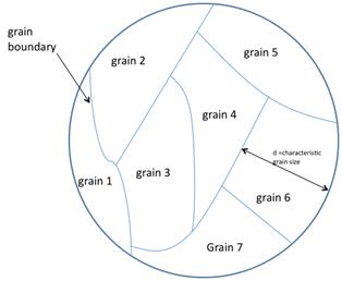
Recombination, which is a limiting factor for current in a solar cell, occurs more prevalently at grain boundaries, see figure 1.
The use of polycrystalline silicon in the production of solar cells requires less material and therefore provides higher profits and increased manufacturing throughput.
[26] The issue of efficiency versus cost is a value decision of whether one requires an "energy dense" solar cell or sufficient area is available for the installation of less expensive alternatives.
[30] As of 2010, as established producers (mentioned below) expand their capacities, additional newcomers – many from Asia – are moving into the market.
It is yet unclear which companies will be able to produce at costs low enough to be profitable after the steep drop in spot-prices of the last months.
[49] The Chinese government accused United States and South Korean manufacturers of predatory pricing or "dumping".
As a consequence, in 2013 it imposed import tariffs of as much as 57 percent on polysilicon shipped from these two countries in order to stop the product from being sold below cost.
[50] Due to the rapid growth in manufacturing in China and the lack of regulatory controls, there have been reports of the dumping of waste silicon tetrachloride.