Czochralski method
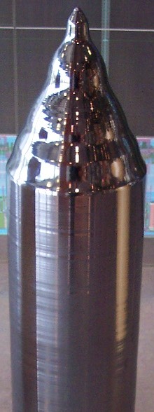
[4] The most important application may be the growth of large cylindrical ingots, or boules, of single crystal silicon used in the electronics industry to make semiconductor devices like integrated circuits.
It is the basic material in the production of integrated circuits used in computers, TVs, mobile phones and all types of electronic equipment and semiconductor devices.
[6] Monocrystalline silicon is also used in large quantities by the photovoltaic industry for the production of conventional mono-Si solar cells.
High-purity, semiconductor-grade silicon (only a few parts per million of impurities) is melted in a crucible at 1,425 °C (2,597 °F; 1,698 K), usually made of quartz.
By precisely controlling the temperature gradients, rate of pulling and speed of rotation, it is possible to extract a large, single-crystal, cylindrical ingot from the melt.
Occurrence of unwanted instabilities in the melt can be avoided by investigating and visualizing the temperature and velocity fields during the crystal growth process.
During growth, the walls of the crucible dissolve into the melt and Czochralski silicon therefore contains oxygen at a typical concentration of 1018 cm−3.
These have the effect of trapping unwanted transition metal impurities in a process known as gettering, improving the purity of surrounding silicon.
Additionally, oxygen impurities can improve the mechanical strength of silicon wafers by immobilising any dislocations which may be introduced during device processing.
[9][10] Therefore, radiation detectors made of Czochralski- and magnetic Czochralski-silicon are considered to be promising candidates for many future high-energy physics experiments.
[11][12] It has also been shown that the presence of oxygen in silicon increases impurity trapping during post-implantation annealing processes.