Printed circuit board manufacturing
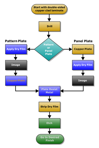
Various techniques, such as silk screening and photoengraving, replicate the desired copper patterns on the PCB layers.
Manufacturing starts from the fabrication data generated by computer aided design, and component information.
CAM performs the following functions: Initially PCBs were designed manually by creating a photomask on a clear mylar sheet, usually at two or four times the true size.
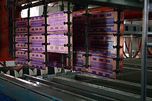
Modern PCBs are designed with dedicated layout software, generally in the following steps:[1][2] Several small printed circuit boards can be grouped together for processing as a panel.
The outer tooling strip often includes tooling holes, a set of panel fiducials, a test coupon, and may include hatched copper pour or similar patterns for even copper distribution over the whole panel in order to avoid bending.
Laser depaneling reduces stress on the fragile circuits, improving the yield of defect-free units.
The first step is to replicate the pattern in the fabricator's CAM system on a protective mask on the copper foil PCB layers.
Small-scale etching requires attention to disposal of used etchant, which is corrosive and toxic due to its metal content.
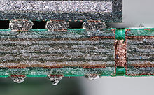
"Undercut" occurs when etchant attacks the thin edge of copper under the resist; this can reduce conductor widths and cause open-circuits.
Where metallic plating is used as a resist, it can "overhang" which can cause short circuits between adjacent traces when closely spaced.
The mask is stripped away and a brief etching step removes the now-exposed bare original copper laminate from the board, isolating the individual traces.
This is achieved by laminating a stack of materials in a press by applying pressure and heat for a period of time.
Holes may be made conductive, by electroplating or inserting hollow metal eyelets, to connect board layers.
When vias with a diameter smaller than 76.2 micrometers are required, drilling with mechanical bits is impossible because of high rates of wear and breakage.
For multi-layer boards, those with three layers or more, drilling typically produces a smear of the high temperature decomposition products of bonding agent in the laminate system.
The de-smear process ensures that a good connection is made to the copper layers when the hole is plated through.
On high reliability boards a process called etch-back is performed chemically with a potassium permanganate based etchant or plasma etching.
Proper plating or surface finish selection can be critical to process yield, the amount of rework, field failure rate, and reliability.
Electrochemical migration (ECM) is the growth of conductive metal filaments on or in a printed circuit board (PCB) under the influence of a DC voltage bias.
Silver also grows conducting surface paths in the presence of halide and other ions, making it a poor choice for electronics use.
Reflow to melt solder or tin plate to relieve surface stress lowers whisker incidence.
[24] A photo-sensitive coating is applied to the surface of the PWB, then exposed to light through the solder mask image film, and finally developed where the unexposed areas are washed away.
There are three methods to print the legend: Boards with no components installed are usually bare-board tested for "shorts" and "opens".
[citation needed] For high-volume testing, a rigid needle adapter makes contact with copper lands on the board.
[25] The fixture or adapter is a significant fixed cost and this method is only economical for high-volume or high-value production.
Or, even if all components are available in through-hole packages, it might be desired to take advantage of the size, weight, and cost reductions obtainable by using some available surface-mount devices.
Another reason to use both methods is that through-hole mounting can provide needed strength for components likely to endure physical stress (such as connectors that are frequently mated and demated or that connect to cables expected to impart substantial stress to the PCB-and-connector interface), while components that are expected to go untouched will take up less space using surface-mount techniques.
PCBs intended for extreme environments often have a conformal coating, which is applied by dipping or spraying after the components have been soldered.
The chief disadvantage of conformal coatings is that servicing of the board is rendered extremely difficult.
Improper handling techniques might transmit an accumulated static charge through the board, damaging or destroying components.