Adatom
[2] If crystallography is used, or if the growth temperatures are higher, which would give an entropy effect, the crystal surface becomes rough, causing greater number of kinks.
This means that adatoms have a greater chance of arriving at a kink site, to become part of the crystal.
[2] The opposite, so with a lower growth temperature, would give a smooth surface, which means that there is a higher number of terrace adsorption sites.
If the adatom-surface interaction is the strongest, the adatoms are more likely to arrange themselves in such a way as to create layers on the surface.
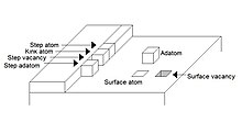
These surfaces have a geometry with vicinal steps separated by "atomically flat low-index terraces".
[2] In some cases the cycle of making new layers in layer-by-layer growth is broken by kinetic constraints.
The more bonds created, the more energy is confined, making it harder to desorb the adatom.
[6] A special site for an adatom is a kink, where exactly half of the bonds with the surface can be created, also called the "half-crystal position".
[7] Adatoms, due to having fewer bonds than the other atoms in the crystal, have unbound electrons.
The structure of the adatoms on a surface can be adjusted by changing the external magnetic field.
[8] The magnetic field created by an atom is caused mostly by the orbit and spin of the electrons.
The proton's and neutron's magnetic moment are negligible when compared to that of the electron due to their larger masses.
This is why bound electrons do not display this magnetic moment, they already have a favorable energy state and it is unfavorable to change.
The magnetization of an (magnetically aligned) atom is given by: Where N is the number of electrons, gj is the g-factor, μB is the Bohr magneton, kB is the Boltzmann constant, T is the temperature and j is the total angular momentum quantum number.
The movement of adatoms across a surface can be described by the Burton–Cabrera–Frank (CBF) model by Keith Burton, Nicolás Cabrera and Charles Frank.
[2] The CBF model obeys the following continuity equation: Combining the steady states (
) with the following boundary conditions can lead to an expression for the velocity of the adatoms at each adsorption site.
Thus, the mapping of the dopant substances will give exact characteristics of any given semiconductor device, once all is known.
[9] With the technology available nowadays it is possible to create a linear chain of adatoms on top of an epitaxial film.
Furthermore, Usami et al. were able to create quantum wells by adding Si atoms to a SiGe bulk crystal.