Epitaxy
For most epitaxial growths, the new layer is usually crystalline and each crystallographic domain of the overlayer must have a well-defined orientation relative to the substrate crystal structure.
In the simplest case, the epitaxial layer can be a continuation of the same semiconductor compound as the substrate; this is referred to as homoepitaxy.
This technology is often used to grow a more pure film than the substrate and to fabricate layers with different doping levels.
is larger than that, the film experiences a volumetric strain that builds with each layer until a critical thickness.
With increased thickness, the elastic strain in the film is relieved by the formation of dislocations, which can become scattering centers that damage the quality of the structure.
Heteroepitaxy is commonly used to create so-called bandgap systems thanks to the additional energy caused by de deformation.
In 2D crystal heterostructure, graphene nanoribbons embedded in hexagonal boron nitride[8][9] give an example of pendeo-epitaxy.
The epitaxial overlayer then creates specific textures along each grain of the seed layer, due to lattice matching.
Epitaxy is used in silicon-based manufacturing processes for bipolar junction transistors (BJTs) and modern complementary metal–oxide–semiconductors (CMOS), but it is particularly important for compound semiconductors such as gallium arsenide.
Manufacturing issues include control of the amount and uniformity of the deposition's resistivity and thickness, the cleanliness and purity of the surface and the chamber atmosphere, the prevention of the typically much more highly doped substrate wafer's diffusion of dopant to the new layers, imperfections of the growth process, and protecting the surfaces during manufacture and handling.
Practical epitaxial growth, however, takes place in a high supersaturation regime, away from thermodynamic equilibrium.
[11] Homoepitaxial growth of semiconductor thin films are generally done by chemical or physical vapor deposition methods that deliver the precursors to the substrate in gaseous state.
This reaction is reversible, and the growth rate depends strongly upon the proportion of the two source gases.
[13] A common technique used in compound semiconductor growth is molecular beam epitaxy (MBE).
In this method, a source material is heated to produce an evaporated beam of particles, which travel through a very high vacuum (10−8 Pa; practically free space) to the substrate and start epitaxial growth.
Liquid-phase epitaxy (LPE) is a method to grow semiconductor crystal layers from the melt on solid substrates.
Centrifugal liquid-phase epitaxy is used commercially to make thin layers of silicon, germanium, and gallium arsenide.
[18] Centrifugal LPE has the capability to create dopant concentration gradients while the solution is held at constant temperature.
The annealing step used to recrystallize or heal silicon layers amorphized during ion implantation is also considered to be a type of solid phase epitaxy.
The impurity segregation and redistribution at the growing crystal-amorphous layer interface during this process is used to incorporate low-solubility dopants in metals and silicon.
[23] An epitaxial layer can be doped during deposition by adding impurities to the source gas, such as arsine, phosphine, or diborane.
Dopants in the source gas, liberated by evaporation or wet etching of the surface, may also diffuse into the epitaxial layer and cause autodoping.
Doping can also be achieved by a site-competition technique, where the growth precursor ratios are tuned to enhance the incorporation of vacancies, specific dopant species or vacant-dopant clusters into the lattice.
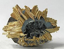
[27] If the crystals of both minerals are well formed so that the directions of the crystallographic axes are clear then the epitaxic relationship can be deduced just by a visual inspection.
In this packing the close-packed layers are parallel to (111) (a plane that symmetrically "cuts off" a corner of a cube).
The hematite structure is based on close-packed oxygen anions stacked in an AB-AB sequence, which results in a crystal with hexagonal symmetry.
Indeed, epitaxy is the only affordable method of high quality crystal growth for many semiconductor materials.