Crystallographic defects in diamond
Such defects may be the result of lattice irregularities or extrinsic substitutional or interstitial impurities, introduced during or after the diamond growth.
The defects can be detected by different types of spectroscopy, including electron paramagnetic resonance (EPR), luminescence induced by light (photoluminescence, PL) or electron beam (cathodoluminescence, CL), and absorption of light in the infrared (IR), visible and UV parts of the spectrum.
The absorption spectrum is used not only to identify the defects, but also to estimate their concentration; it can also distinguish natural from synthetic or enhanced diamonds.
In diamond, only defects of the following symmetries have been observed thus far: tetrahedral (Td), tetragonal (D2d), trigonal (D3d, C3v), rhombic (C2v), monoclinic (C2h, C1h, C2) and triclinic (C1 or CS).
[2] In synthetic diamond grown by the high-pressure high-temperature synthesis[5] or chemical vapor deposition,[6][7] defects with symmetry lower than tetrahedral align to the direction of the growth.
[16] Absorption of light and other material properties of diamond are highly dependent upon nitrogen content and aggregation state.
Light with energy above ~2.2 eV can excite the donor electrons into the conduction band, resulting in the yellow color.
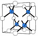
[22] The A center is diamagnetic, but if ionized by UV light or deep acceptors, it produces an electron paramagnetic resonance spectrum W24, whose analysis unambiguously proves the N=N structure.
Spectroscopists use the whole spectrum rather than one peak for defect identification and consider the history of the growth and processing of individual diamond.
This important property of phosphorus in diamond favors electronic applications, such as UV light-emitting diodes (LEDs, at 235 nm).
Those films are produced by various chemical vapor deposition (CVD) techniques in an atmosphere rich in hydrogen (typical hydrogen/carbon ratio >100), under strong bombardment of growing diamond by the plasma ions.
Within the diamond lattice itself, hydrogen-vacancy[37] and hydrogen-nitrogen-vacancy[38] complexes have been identified in negative charge states by electron paramagnetic resonance.
[45] This fact is by all means unusual considering the large difference in size between carbon and transition metal atoms and the superior rigidity of the diamond lattice.
[2][45] Numerous Ni-related defects have been detected by electron paramagnetic resonance,[5][46] optical absorption and photoluminescence,[5][46] both in synthetic and natural diamonds.
Its production mechanism is generally accepted as follows: large nickel atom incorporates substitutionally, then expels a nearby carbon (creating a neighboring vacancy), and shifts in-between the two sites.
Several defects related to isolated cobalt have been detected by electron paramagnetic resonance[50] and photoluminescence,[5][51] but their structure is yet unknown.
A chromium-related optical center was reported after ion implantation and subsequent annealing of Type IIA synthetic diamonds.
[55] Isolated silicon defects have been detected in diamond lattice through the sharp optical absorption peak at 738 nm[56] and electron paramagnetic resonance.
[57] Similar to other large impurities, the major form of silicon in diamond has been identified with a Si-vacancy complex (semi-divacancy site).
[59] Germanium, tin and lead are normally absent in diamond, but they can be introduced during the growth or by subsequent ion implantation.
[62] Similar to N-V centers, Si-V, Ge-V, Sn-V and Pb-V complexes all have potential applications in quantum computing.
[63][61] Around the year 2000, there was a wave of attempts to dope synthetic CVD diamond films by sulfur aiming at n-type conductivity with low activation energy.
So far (2009), there is only one reliable evidence (through hyperfine interaction structure in electron paramagnetic resonance) for isolated sulfur defects in diamond.
The corresponding center called W31 has been observed in natural type-Ib diamonds in small concentrations (parts per million).
When it meets other interstitials it aggregates into larger complexes of two and three split-interstitials, identified by electron paramagnetic resonance (R1 and O3 centers),[70][71] optical absorption and photoluminescence.
[76] Upon annealing of pure diamond at ~700 °C, vacancies migrate and form divacancies, characterized by optical absorption and electron paramagnetic resonance.
Similar mechanism (vacancy aggregation) is also believed to cause brown color of plastically deformed natural diamonds.
The dislocations produce dangling bonds which introduce energy levels into the band gap, enabling the absorption of light.
Boron interacts with carbon interstitials forming a neutral boron–interstitial complex with a sharp optical absorption at 0.552 eV (2250 nm).
[97] The assumed mechanism is trapping of migrating vacancy by substitutional silicon resulting in the Si-V (semi-divacancy) configuration.